Die thinning methods

a technology of thinning methods and dies, applied in the direction of basic electric elements, semiconductor/solid-state device manufacturing, electric apparatus, etc., can solve the problems of power, size, weight, and weight, and the need for compact packaging of electronic components, and the complexity of electronic systems

Inactive Publication Date: 2005-03-01
UNION SEMICON TECH
View PDF2 Cites 82 Cited by
  • Summary
  • Abstract
  • Description
  • Claims
  • Application Information

AI Technical Summary

Benefits of technology

It is therefore a further object of the invention to provide novel methods that, after the back grinding tape has been cured and while it maintains a force of 5 g/25 mm applied to a top surface of the die, the back grinding tape and die are placed face down on a manual tape station and a transfer tape is then applied to

Problems solved by technology

As electronic systems grow in complexity, the need for compact packaging of electronic components increases.
Furthermore, with increasing complexity, other factors, su

Method used


Image

  • Die thinning methods
  • Die thinning methods
  • Die thinning methods

Examples


Embodiment Construction

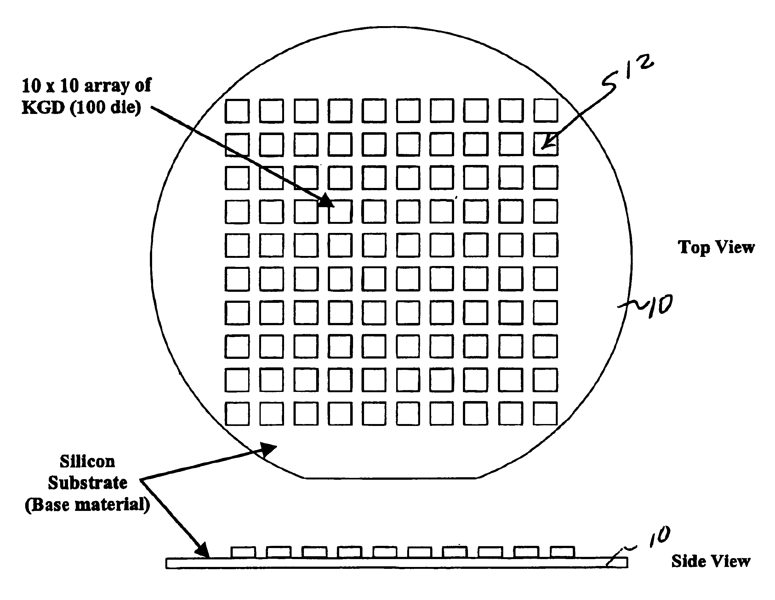
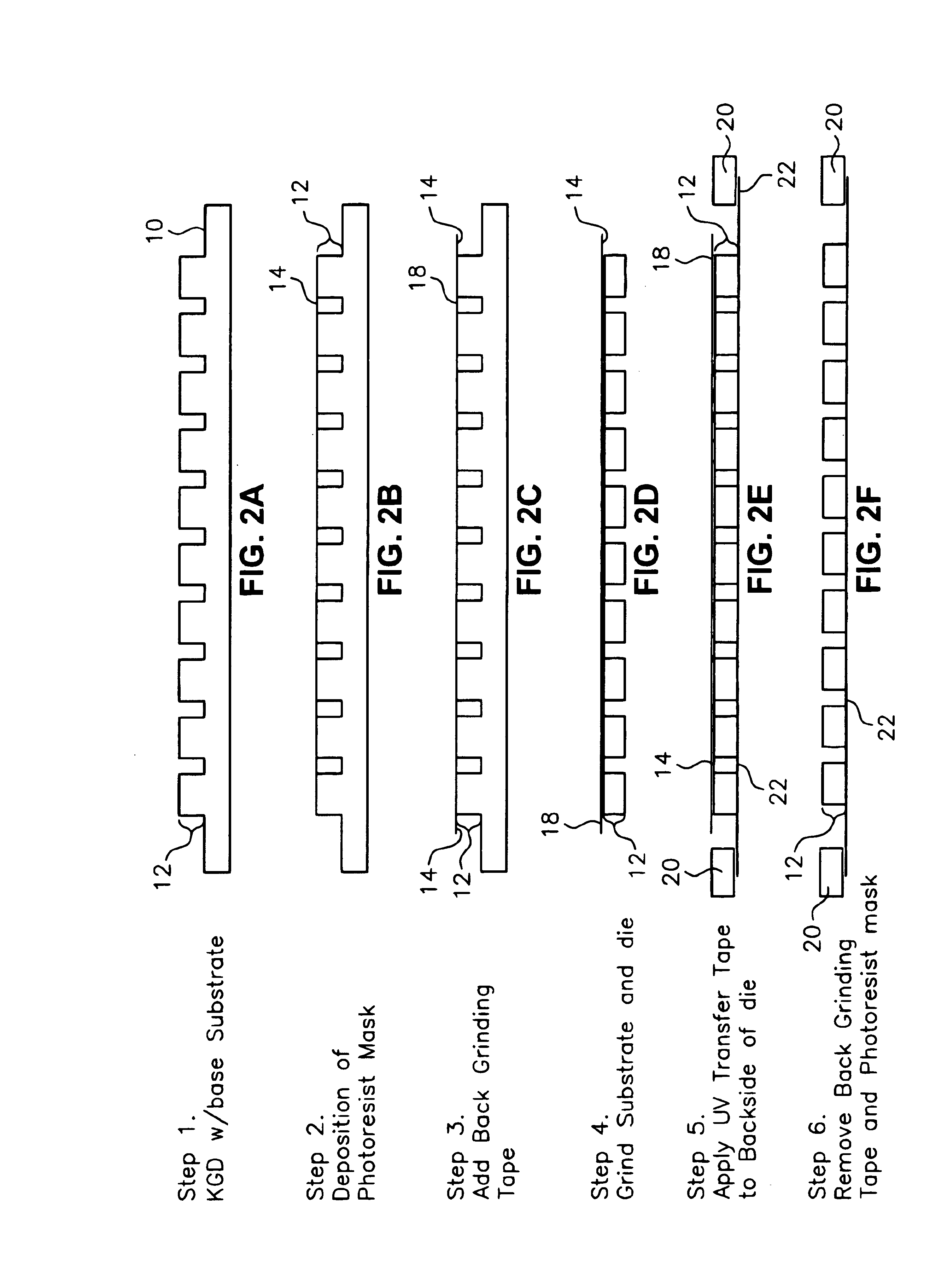
Provisions are suitably provided to provide a method to thin a known good die 12 also known as the known good die 12 thinning process. According to the preferred teachings of the present invention the known good die 12 thinning process reduces known good die 12 from a full thickness of 26 mils down to 5 mils, or other reduced dimension, by using a dielectric deposition, pick and place, and grinding processes. The process was developed to reduce the thickness on individual known good die 12, and not an entire six, eight or twelve inch wafer.

A known good die is classified as a fully functional integrated circuit (IC) used in the microelectronics industry. A die is also known as an integrated circuit (IC), or chip. A thinning Process is a process that reduces the die thickness from full to a reduced thickness. In one example embodiment, die thickness is reduced from 26 to 5 mils. A die pick and place process is a process that utilizes a pick and place tool to place die 12 at predetermi...


PUM


Abstract

A die thinning method includes providing a wafer (10) and depositing a substrate bonding material on the wafer. The die thinning method places a plurality of die (12) on the wafer (10), cures the substrate bonding material to secure the individual ICs to the base wafer (10), and covers the substrate (10) and the die (12) with a mask material. The substrate bonding material is BCB. The mask material is a photoresist (14). The method further back grinds the wafer to remove the wafer and to reduce the original die thickness from 26 mils to 5 mils. A UV transfer tape (22) is applied to the die (12) on a film frame (20). The mask material and back grinding tape (18) are then removed. The plurality of die (12), UV transfer tape (22), and film frame (20) are placed face down in a UV cure station. The UV transfer tape (22) is UV irradiated and the plurality of die (12) are removed from the UV transfer tape (22).

Description

The present invention generally relates to apparatus and methods for thinning dies, and more particularly to apparatus and methods for thinning dies to make magnetic random access memory.BACKGROUND OF THE INVENTIONAs electronic systems grow in complexity, the need for compact packaging of electronic components increases. Furthermore, with increasing complexity, other factors, such as power, size, and weight, require consideration. Thin die, or chips, allow for more compact packaging of electronic components. Thin die are particularly useful in multiple chip packages, providing for packaging of a greater number of die within the same volume. These multiple chip packages often employ three-dimensional packaging technologies, by stacking chips, or die, along the z-axis.Techniques that reduce structural strain on the die during processing would allow the use of thin die.Fabricating thin die in multiple chip modules would provide further advantages for compact packaging of electronic com...

Claims


Application Information

Patent Timeline
IPC IPC(8): H01L21/02H01L21/304H01L21/301H01L21/78
CPCH01L21/78H01L21/304
Inventor HAMPTON, KEVIN WADE
Owner UNION SEMICON TECH
Why Eureka
Try Eureka