

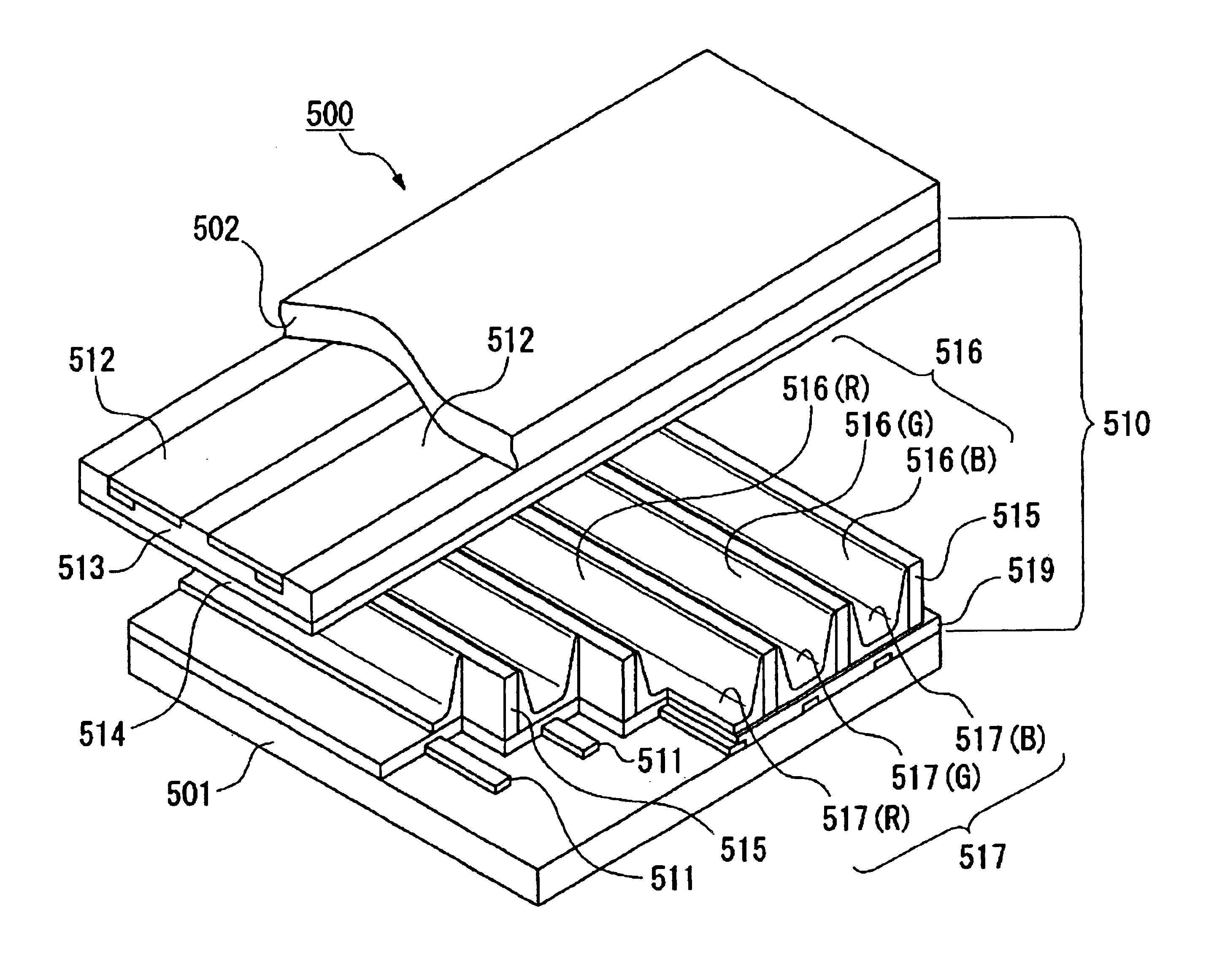
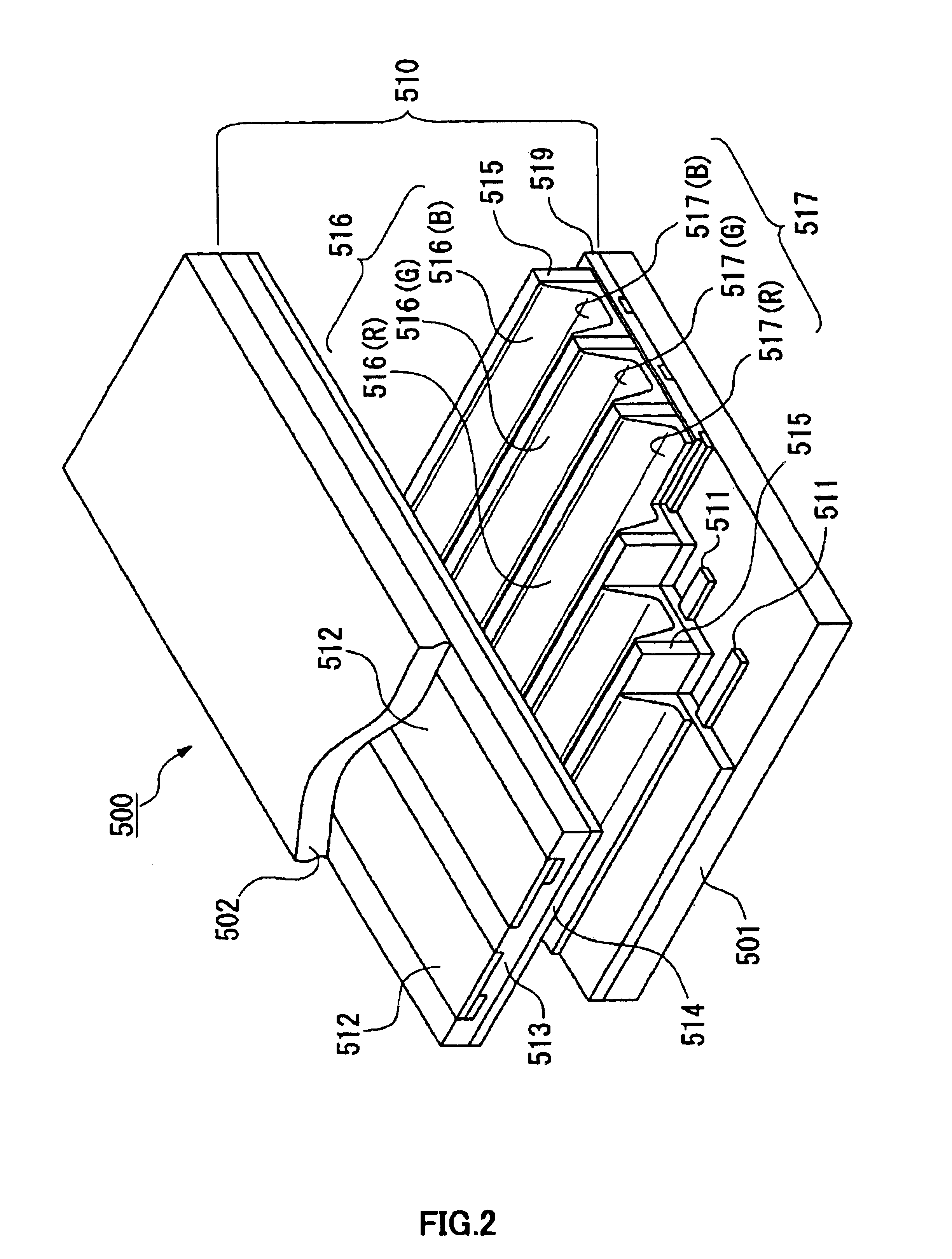
Surface treatment method, surface-treated substrate, method for forming film pattern, method for making electro-optical device, electro-optical device, and electronic apparatus
a surface treatment and substrate technology, applied in the direction of loop antennas, transistors, resonant antennas, etc., can solve the problems of difficult to achieve desired lyophobicity and difficult to set the contact angle between liquid and substrate at less than 70 deg
- Summary
- Abstract
- Description
- Claims
- Application Information
AI Technical Summary
Benefits of technology
Problems solved by technology
Method used
Image

Examples
first exemplary embodiment
[First Exemplary Embodiment]
In a first exemplary embodiment, a surface treatment method of the present invention is described. The surface treatment method in this exemplary embodiment includes a lyophobic treatment step and a lyophilic treatment step. The individual steps are described below.
(Lyophobicity-Imparting Treatment)
In a lyophobic treatment method, a self-assembled layer including an organic molecular film is formed on a surface of a substrate.
An organic molecular film to treat a surface of a substrate contains, at one end, functional groups that are linkable to the substrate, at the other end, functional groups that modify the surface properties of the substrate such that the surface is lyophobic (i.e., control the surface energy), and straight carbon chains or partially branched carbon chains that combine the functional groups on both ends together. The organic molecular film links to the substrate and self-assembles to form a molecular film, such as a monomolecular laye...
second exemplary embodiment
[Second Exemplary Embodiment]
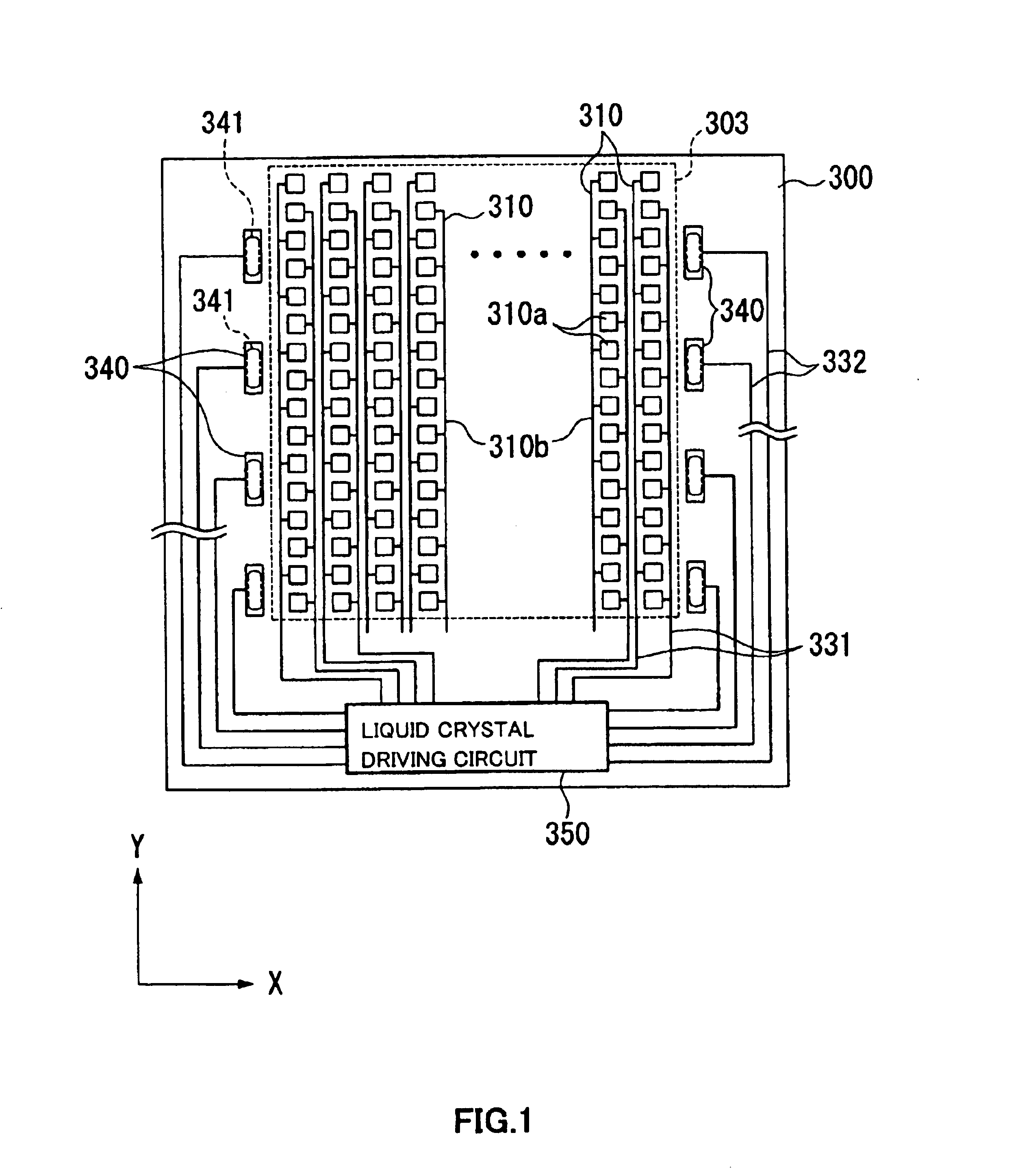
In a second exemplary embodiment, a method of forming wiring, which is an example of the method for forming the film pattern of the present invention, is described below. The method of forming wiring in this exemplary embodiment includes surface treatment, discharge, and heat treatment / phototreatment. The individual steps are described below.
(Surface Treatment)
As the substrate on which wiring composed of a conductive film is formed, a substrate composed of various types of materials may be used, such as a Si wafer, quartz glass, glass, a plastic film, and a metal sheet.
The substrate composed of such a material on which a semiconductor film, metal film, dielectric film, organic film, or the like, is formed as an underlayer may be used as the substrate to form the conductive wiring film.
Surface treatment is performed by the method in accordance with the first exemplary embodiment on the surface of the substrate to form the conductive wiring film so that th...
third exemplary embodiment
[Third Exemplary Embodiment]
In a third exemplary embodiment, a method of forming a silicon film pattern, which is an example of the method for forming the film pattern of the present invention, is described below. The method of forming the silicon film pattern in this exemplary embodiment includes surface treatment, discharge, and heat treatment / phototreatment. The individual steps are described below.
(Surface Treatment)
As the substrate on which a silicon thin-film pattern is formed, a substrate composed of various types of materials may be used, such as a Si wafer, quartz glass, glass, a plastic film, and a metal sheet. The substrate composed of such a material on which a semiconductor film, metal film, dielectric film, organic film, or the like, is formed as an underlayer may also be used as the substrate to form the silicon thin-film pattern.
The surface of the substrate to form the silicon thin-film pattern is subjected to surface treatment by the method in accordance with the fi...
PUM
 Abstract
Description
Claims
Application Information