Magnetic field sensor

a magnetic field sensor and sensor technology, applied in the field can solve the problems of large chip area occupied by output parts, large circuit scale for cancelling input offset voltage, and large consumption current reduction of magnetic field sensors, etc., and achieve the effect of large gain of voltage amplifiers

Inactive Publication Date: 2005-03-01
COLLABO INNOVATIONS INC
View PDF7 Cites 12 Cited by
  • Summary
  • Abstract
  • Description
  • Claims
  • Application Information

AI Technical Summary

Benefits of technology

When the resistance value of a Hall element is small, the resistance value of the resistance made of this identical element becomes small and the magnetic field sensor is configured so that the gain of the voltage amplifier becomes small as a result. On the contrary, when the resistance value of the Hall element is large, the resist

Problems solved by technology

When the double output-type amplifier is used, however, the output part has a large number of component elements and a large chip area is occupied.
In a conventional configuration, there is the defect that the circuit scale for canceling the input offset voltage is large.
In addition, a magnetic field sensor has been used in products which are battery operated, such as cellular phones,

Method used


Image

  • Magnetic field sensor
  • Magnetic field sensor
  • Magnetic field sensor

Examples


embodiment 1

<<Embodiment 1>>

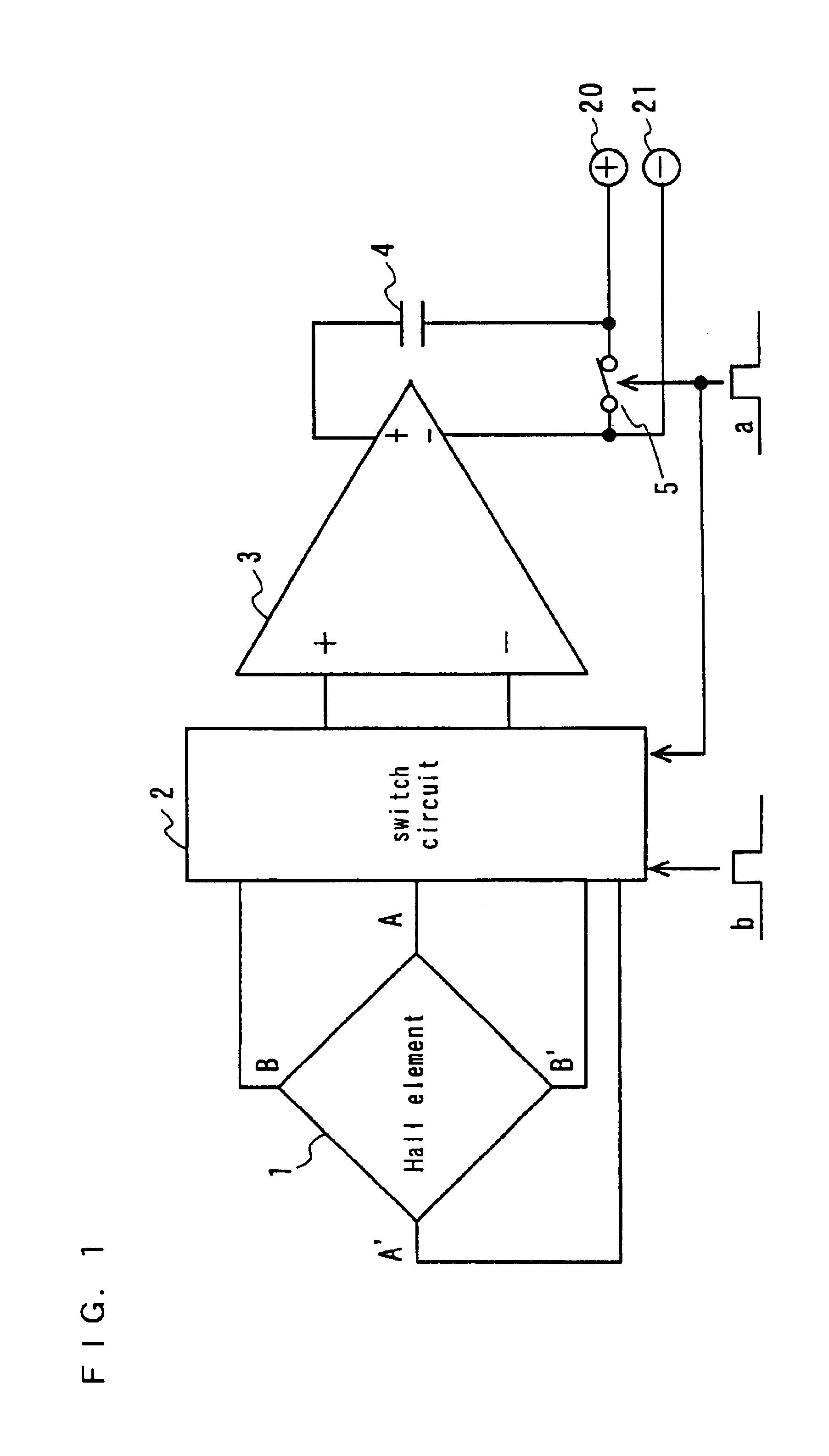
FIG. 1 shows a configuration of a magnetic field sensor according to the first embodiment of the present invention. In FIG. 1, a Hall element is denoted as 1, a switch circuit is denoted as 2, a voltage amplifier is denoted as 3, a capacitor which is a memory element is denoted as 4 and a switch is denoted as 5.

The Hall element 1 is a Hall element in a plate form with four terminals, and the form of the Hall element 1 is geometrically equivalent.

The first phase signal (a) that has a pulse in the first phase is given to the switch 5 and the switch circuit 2. The second phase signal (b) that has a pulse in the second phase is given to the switch circuit 2.

The timing chart in the first embodiment is shown in FIG. 7.

With respect to the magnetic field sensor constructed as the above, the operation is described in the following.

The operation of the first phase is described.

In the first phase, the switch 5 is closed.

At this time, a power source voltage is applied ...

embodiment 2

<<Embodiment 2>>

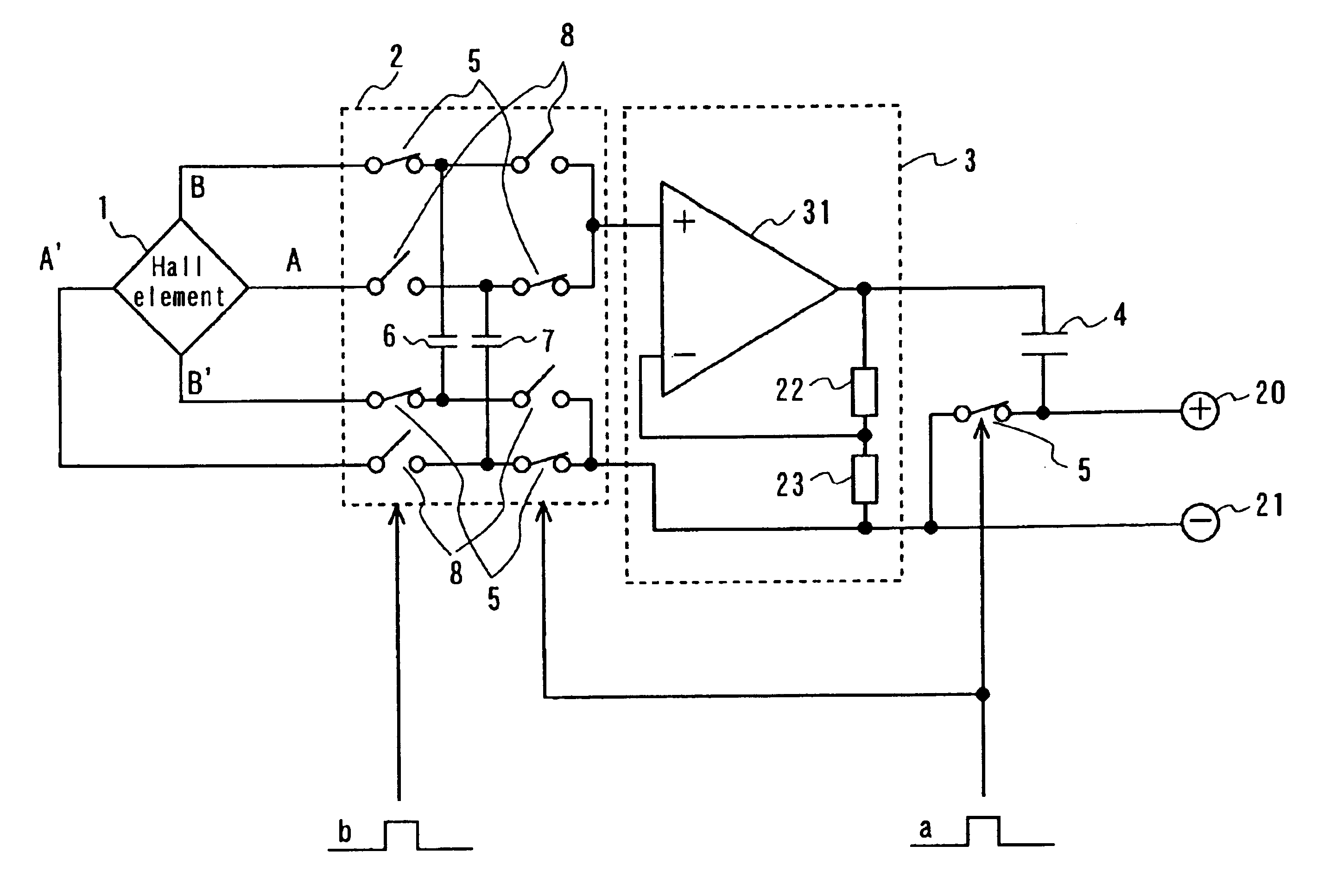
FIG. 2 shows a configuration of a magnetic field sensor according to the second embodiment of the present invention. In FIG. 2 a Hall element is denoted as 1, a switch circuit is denoted as 2, a voltage amplifier is denoted as 3, capacitors which are memory elements are denoted as 4, 6 and 7, and switches are denoted as 5 and 8.

The Hall element 1 is a Hall element in a plate form with four terminals, and the form of the Hall element 1 is geometrically equivalent.

The voltage amplifier 3 is formed of a single input amplifier and two resistances 22, 23 which define the amplification factor (feed back amount). This is the same as the voltage amplifier 3 of the first embodiment with respect to the function which outputs a voltage proportional to the input voltage.

In the first phase, the first phase signal (a) which has a pulse is given to the switch 5 (including the switch 5 which forms a part of the switch circuit 2) and a changing switch of a circuit which app...

embodiment 3

<<Embodiment 3>>

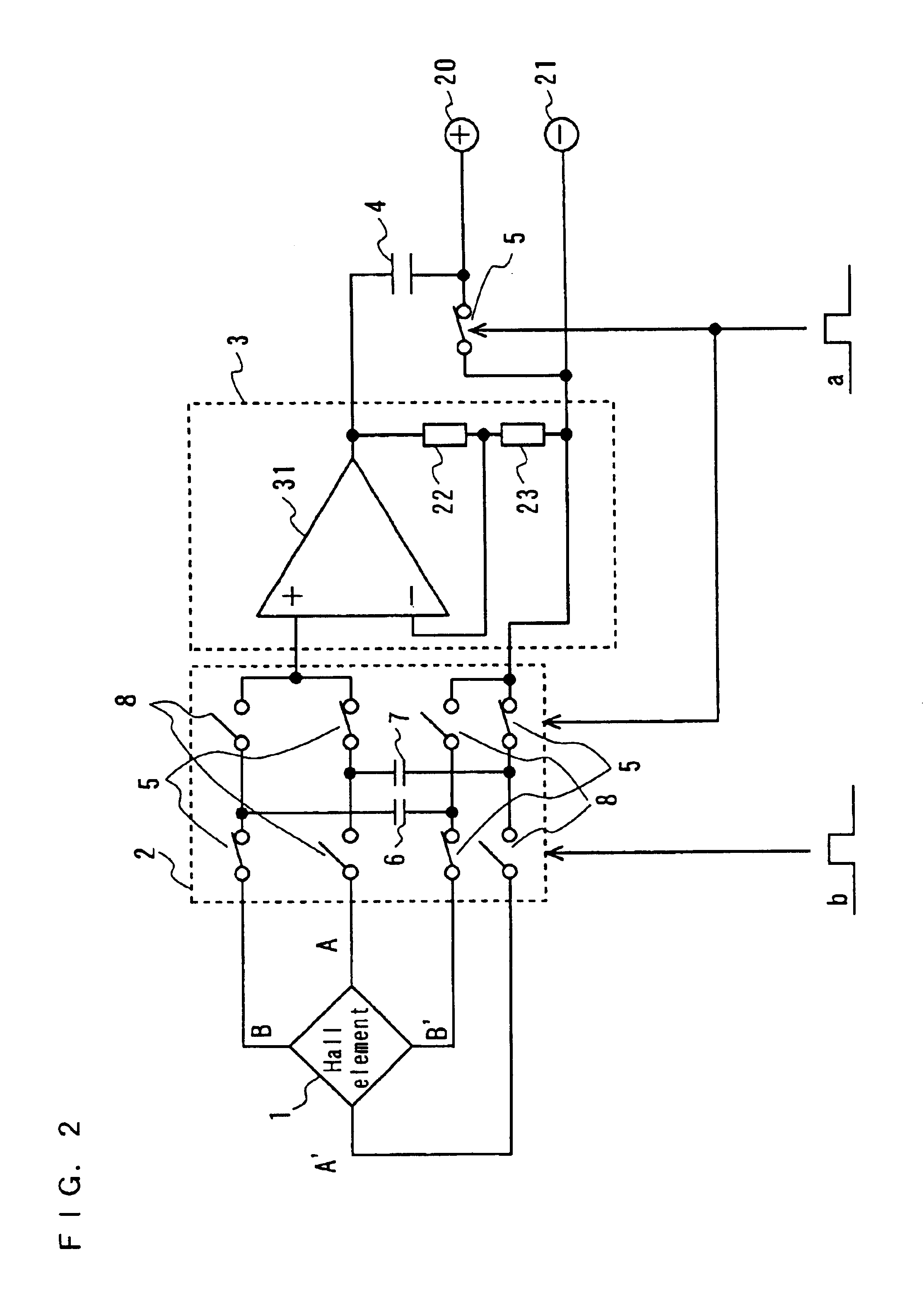
FIG. 3 illustrates a magnetic field sensor of the third embodiment which uses the magnetic field sensor of the first embodiment according to the present invention. The magnetic field sensor of the third embodiment outputs a binary digital signal of 0 or 1 in accordance with the intensity of the magnetic field.

In FIG. 3, a Hall element is denoted as 1, a switch circuit is denoted as 2, a voltage amplifier is denoted as 3, a capacitor which is a memory element is denoted as 4, a switch (which is closed in the first phase and is open in the other phase) is denoted as 5, a comparator is denoted as 13, a latch circuit is denoted as 14, a clock generation circuit is denoted as 15, the first phase clock generation circuit is denoted as 16 and the second phase clock generation circuit is denoted as 17.

The Hall element 1 has a plate form with four terminals, and the form of the Hall element 1 is geometrically equivalent.

(a) in FIG. 7 shows a waveform (including the ...


PUM


Abstract

A magnetic field sensor including an amplifier and a magnetic field element for outputting a signal to a switch circuit according to the strength of an applied magnetic field. The switch circuit outputs a signal selected by an external two-phase signal to an amplifier that amplifies the signal and outputs a resulting voltage to a first end of a memory element. A switch, having one end connected to a second end of the memory element, is controlled by the two-phase signal. The switch closes in a first phase of the two-phase signal causing the memory element to store the output voltage of the amplifier, and opens in a second phase causing a vector sum of the output voltage the amplifier to be stored in the memory element and providing the output voltage to a signal output terminal connected to the second end of the memory element.

Description

BACKGROUND OF THE INVENTIONThe present invention relates to a magnetic field sensor which comprises a Hall element and an amplifier for amplifying the output voltage of the Hall element and which detects the magnetic field strength in the installed location so as to output a signal in accordance with the detected magnetic field strength.A typical magnetic field sensor is a bipolar IC or a CMOS IC which include a Hall element for outputting an output voltage proportional to the magnetic field strength and an amplifier for amplifying an output voltage of the Hall element as well as a comparator for inputting the output voltage of the amplifier to be compared with a reference potential and for outputting the comparison result. Such a magnetic field sensor outputs an output signal of two values (0 or 1) showing whether the magnetic field strength of the location where the magnetic field sensor is installed is larger or smaller than a constant reference.Another magnetic field sensor comp...

Claims


Application Information

Patent Timeline
IPC IPC(8): G01R33/06G01R33/07
CPCG01R33/07
Inventor HARA, JUN-ICHIROHATANAKA, TADATA
Owner COLLABO INNOVATIONS INC
Why Eureka
Try Eureka