High speed interface for a programmable interconnect circuit

a high-speed interface and interconnecting circuit technology, applied in the field of programmable semiconductor circuits, can solve the problems of co-channel interference and emi effects of parallel data transmission, the number of fuses in the resulting global routing pool becomes prohibitive, and the density of modern boards continues to increas

Inactive Publication Date: 2005-03-01
LATTICE SEMICON CORP
View PDF9 Cites 31 Cited by
  • Summary
  • Abstract
  • Description
  • Claims
  • Application Information

AI Technical Summary

Benefits of technology

The invention will be more fully understood upon consideration of the detailed description below, taken together with the accompanying drawings.

Problems solved by technology

Although this “bit-oriented” architecture allowed a user to programmably interconnect signals through the device, the number of fuses in the resulting global routing pool becomes prohibitive as the pin count increases.
However, modern board density continues to increase, demanding an interconnect device having a suitable number of pins to interconnect the signals.
At the gigabit transmission rate of these applications, parallel data transmission suffers from co-channel interference and EMI effects.
Skew is a big problem for sending parallel data and its clock across cables or PCB traces because the phase relation of the data and clock can be lost as a result of different travel times through the link.
The problem disappears because the clock travels with the data over the same differential pair of wires.
Because bit transitions are absent, the clock recovery component loses or cannot recover the clock during these periods.

Method used


Image

  • High speed interface for a programmable interconnect circuit
  • High speed interface for a programmable interconnect circuit
  • High speed interface for a programmable interconnect circuit

Examples


Embodiment Construction

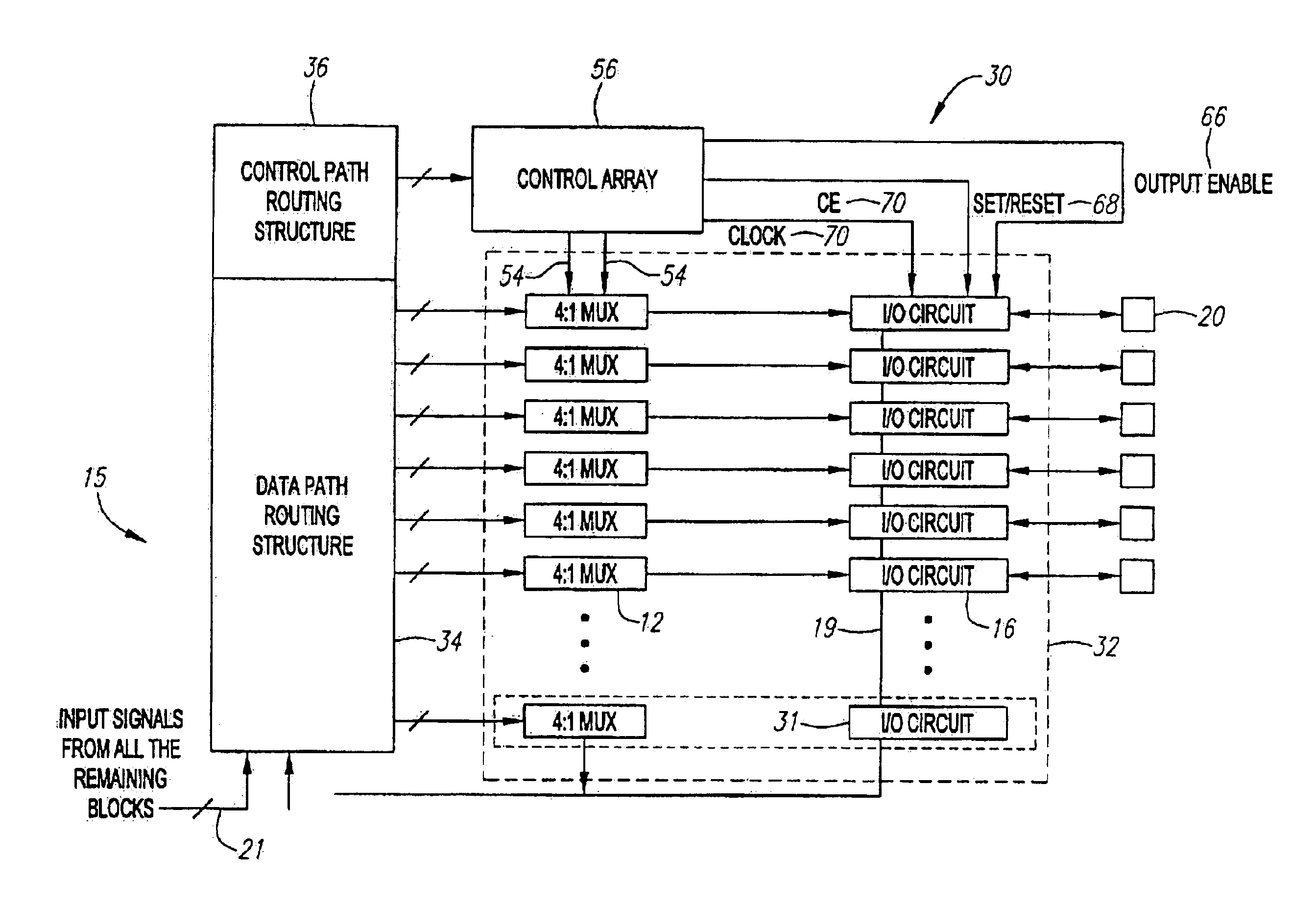
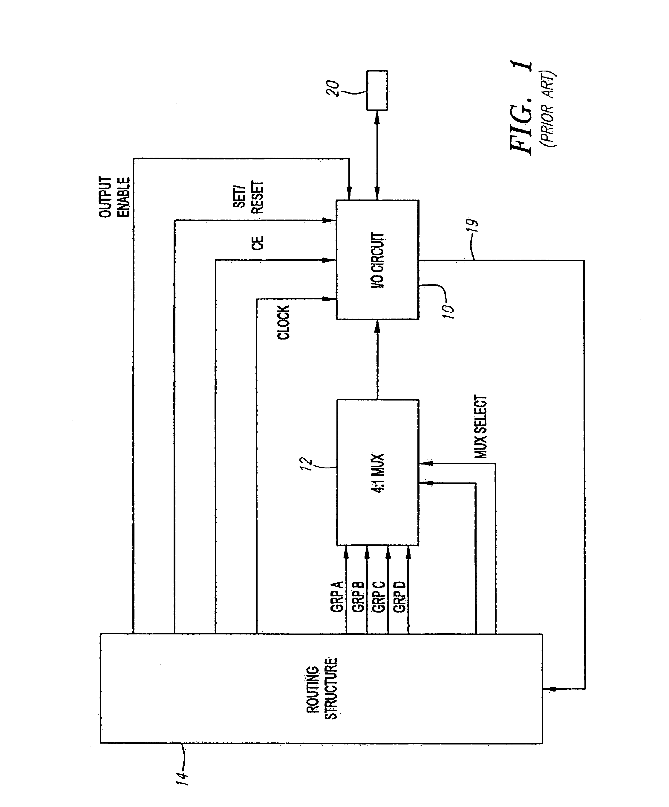
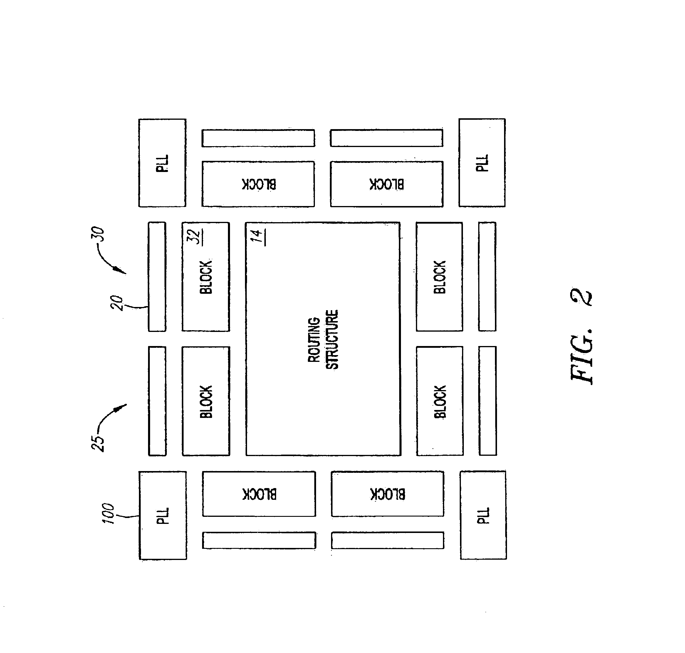
Referring now to FIGS. 2 and 3, a programmable interconnect device 25 having a “block-oriented” architecture 30 is illustrated. In contrast to the “bit-oriented” architecture of the prior art, the I / O circuits 16 (FIG. 3) are arranged in I / O blocks 32 such that each block 32 having a plurality X of I / O circuits 16 associates with its own routing structure 15 (FIG. 3). In general, X is arbitrary as any number of I / O circuits 16 may be assigned to an I / O block 32. However, because bus-switching applications typically route binary signals in groups of 8 (one byte) or 16 (two bytes), assigning 16 I / O circuits per I / O block 32 is particularly convenient. It will be appreciated, however, that other numbers of I / O circuits per I / O block may be used, for example, 4 or 8. Each I / O circuit 16 may be contained within an I / O cell 31, which also includes a 4:1 MUX 12 for selecting data signal inputs for I / O circuit 16. In FIG. 2, the routing structures 15 are collectively denoted as a single rou...


PUM


Abstract

A programmable semiconductor device comprising a plurality of I/O circuits arranged into blocks includes a routing structure for each block, wherein each routing structure may programmably route signals between its block's I/O circuits and the I/O circuits within the remaining blocks. Each I/O circuit associates with a pin such that each block has a set of pins. A SERDES and a FIFO buffer associate with each block. Each block's SERDES couples between the block's I/O circuits and the block's set of pins. Each FIFO buffer couples between the SERDES and its block's I/O circuits.

Description

FIELD OF THE INVENTIONThis invention relates generally to programmable semiconductor circuits, and more particularly to the input and output of data through such a circuit.DESCRIPTION OF RELATED ARTIn-system-programmable interconnect devices permit a user to programmably route signals between pins of the device. For example, Lattice Semiconductor Corp. currently manufactures an ispGDX® family of programmable interconnect devices having a non-volatile E2CMOS® in-system-programmable crossbar switch matrix for programmable switching, interconnect, and jumper functions. Each pin of the ispGDX® device is associated with an input / output (I / O) circuit that programmably couples to other I / O circuits through a routing structure denoted as a global routing pool (GRP). The I / O circuits contain registers allowing the input and output signals on the associated pins to be selectively registered.Referring now to FIG. 1, an input / output circuit 10 for an ispGDX® device couples to a 4:1 multiplexer ...

Claims


Application Information

Patent Timeline
Patent Type & Authority Patents(United States)
IPC IPC(8): H03K19/177H01L21/82
CPCH03K19/17744
Inventor AGRAWAL, OM P.ZHU, JINGHUICHI, KUANGCHEN, CHIENKUANG
Owner LATTICE SEMICON CORP
Why Eureka
Try Eureka