Method for removal of photoresist using sparger

a technology of sparger and photoresist, which is applied in the field of silicon semiconductor manufacturing, can solve the problems of affecting the ability to further process the workpiece, affecting the ability to remove photoresist, and tracing impurities, etc., and achieves the effect of efficient and fast methods of removing photoresis

Inactive Publication Date: 2005-03-08
NAURA AKRION INC
View PDF4 Cites 3 Cited by
  • Summary
  • Abstract
  • Description
  • Claims
  • Application Information

AI Technical Summary

Benefits of technology

to provide an improved apparatus for use in the process which results in and ...

Problems solved by technology

Trace impurities, such as sodium ions, metals, and particles, are especially detrimental if present on semiconductor surfaces during high-temperature processing because they may spread and diffuse into the semiconductor workpiece and thereby alter the electrical characteristics of the devices formed in the workpiece.
Such bonded photo...

Method used


Image

  • Method for removal of photoresist using sparger
  • Method for removal of photoresist using sparger

Examples


Embodiment Construction

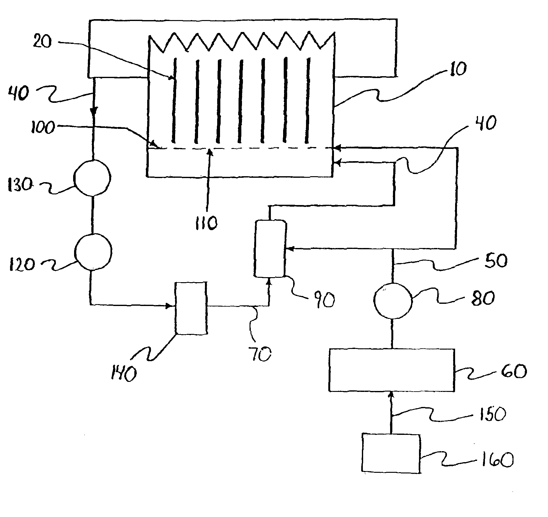
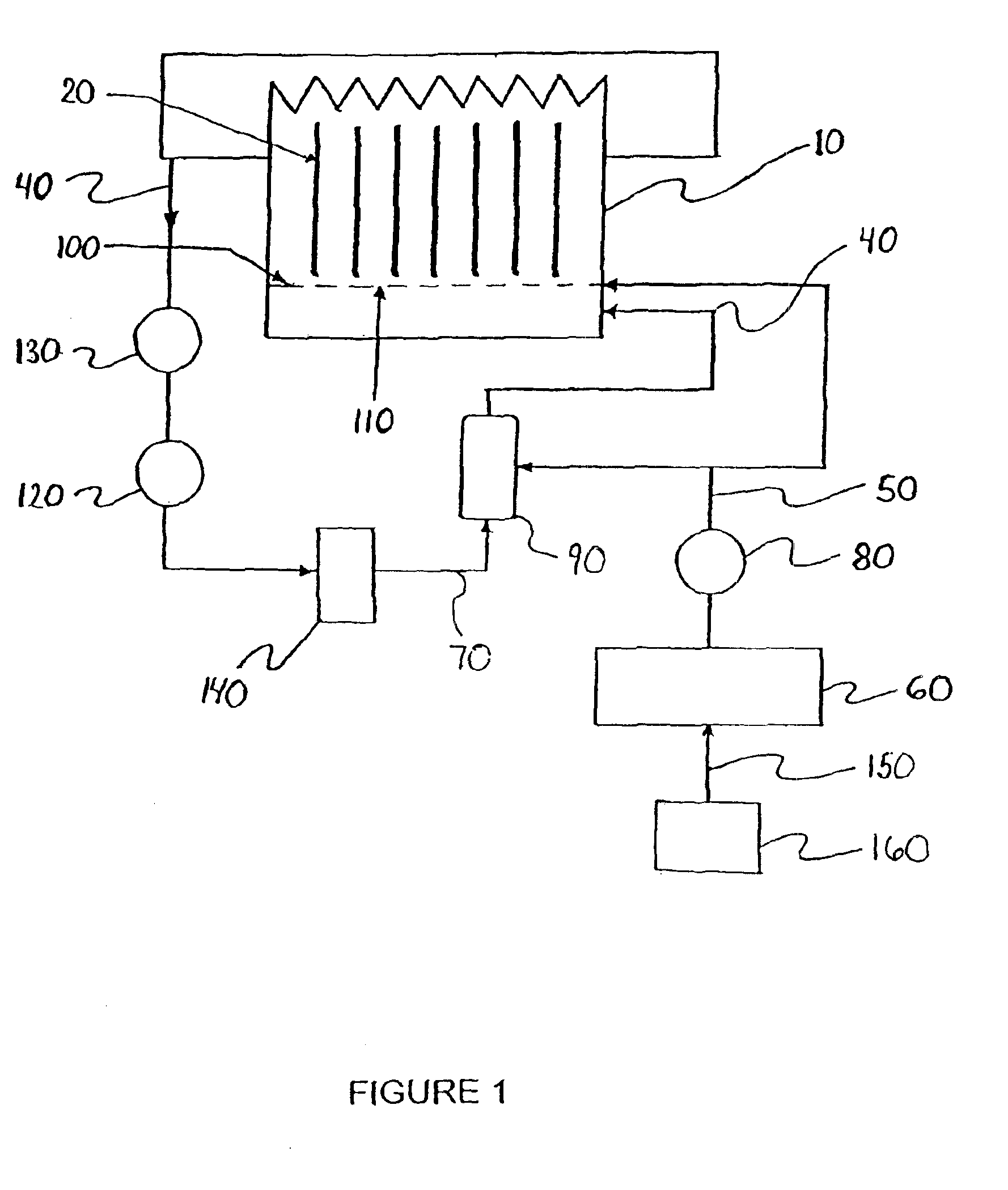
According to the invention, an apparatus is disclosed which includes cassettes filled with semiconductor wafers having a layer or multi-layers of photoresist wherein the semiconductor wafers are exposed to pressurized DIO3 water at ambient temperatures and with a velocity produced by a sparger plate so as to etch or remove the photoresist at a higher rate than previously known.

Preferably the process tank containing the silicon wafers from which photoresist is to be removed or etched contains a fixed amount of DI water at ambient or higher temperature. O3 is generated with a generator. A portion is directed to a pressurized ozonator where it is mixed with DI water and then introduced into the process tank through the sparger, and another portion of the O3 is introduced directly to the sparger plate.

The DIO3 flows from the tank through a sensor, then to a pump, a filter, to the ozonator where it is pressurized, and then back to the pressurized plenum (sparger) at the bottom of the pro...


PUM

PropertyMeasurementUnit
Temperatureaaaaaaaaaa
Concentrationaaaaaaaaaa

Abstract

A method of removing photoresist from semiconductor wafers through the use of a sparger plate. According to the inventive method, at least one semiconductor wafer is positioned in a process tank above the sparger plate. A mixture of ozone and deionized water is introduced into the process tank at a position below the sparger plate. The mixture of ozone and deionized water is then introduced across the wafer via the sparger plate at an increased flow velocity while the wafer is submerged in the mixture of deionized water and ozone.

Description

FIELD OF THE INVENTIONThis invention relates to the field of manufacturing silicon semiconductors, more specifically to processes and apparatus for removing photoresist from the surfaces of silicon semiconductor wafers during such manufacturing.BACKGROUND OF THE INVENTIONThe importance of clean semiconductor workpiece surfaces in the fabrication of semiconductor microelectronic devices has been recognized for a considerable period of time. Over time, as VLSI and ULSI silicon circuit technology has developed, the cleaning processes have gradually become a particularly critical step in the fabrication process. Trace impurities, such as sodium ions, metals, and particles, are especially detrimental if present on semiconductor surfaces during high-temperature processing because they may spread and diffuse into the semiconductor workpiece and thereby alter the electrical characteristics of the devices formed in the workpiece.The actual stripping of photoresist from the workpiece is yet a...

Claims


Application Information

Patent Timeline
IPC IPC(8): G03F7/42
CPCG03F7/423
Inventor NOVAK, RICHARDKASHKOUSH, ISMAIL
Owner NAURA AKRION INC
Why Eureka
Try Eureka