Charge pump device

a technology of a pump and a discharge pump, which is applied in the direction of electric variable regulation, process and machine control, instruments, etc., can solve the problems of reducing the resistance of a charge transfer mos, generating harmonic noise when switching a current, and latching up, so as to achieve high efficiency and large current capacity

Inactive Publication Date: 2005-03-08
SEMICON COMPONENTS IND LLC
View PDF2 Cites 20 Cited by
  • Summary
  • Abstract
  • Description
  • Claims
  • Application Information

AI Technical Summary

Benefits of technology

This invention can solve the issues addressed above, and can realize a charge pump device with large current capacity and high efficiency.

Problems solved by technology

However, it has a drawback to generate a harmonic noise when switching a current.
The first issue is to reduce ON resistance of a charge transfer MOS transistor, so that the charge pump circuit can provide a high voltage (over 10V) and a large current (several milliamperes) required to the power supply circuit.
The second issue is to prevent a latch up, which often happens to a high current charge pump device.
Especially, there has been a problem with a large current charge pump device to cause a latch up at the beginning of the operation.

Method used


Image

  • Charge pump device
  • Charge pump device
  • Charge pump device

Examples


second embodiment

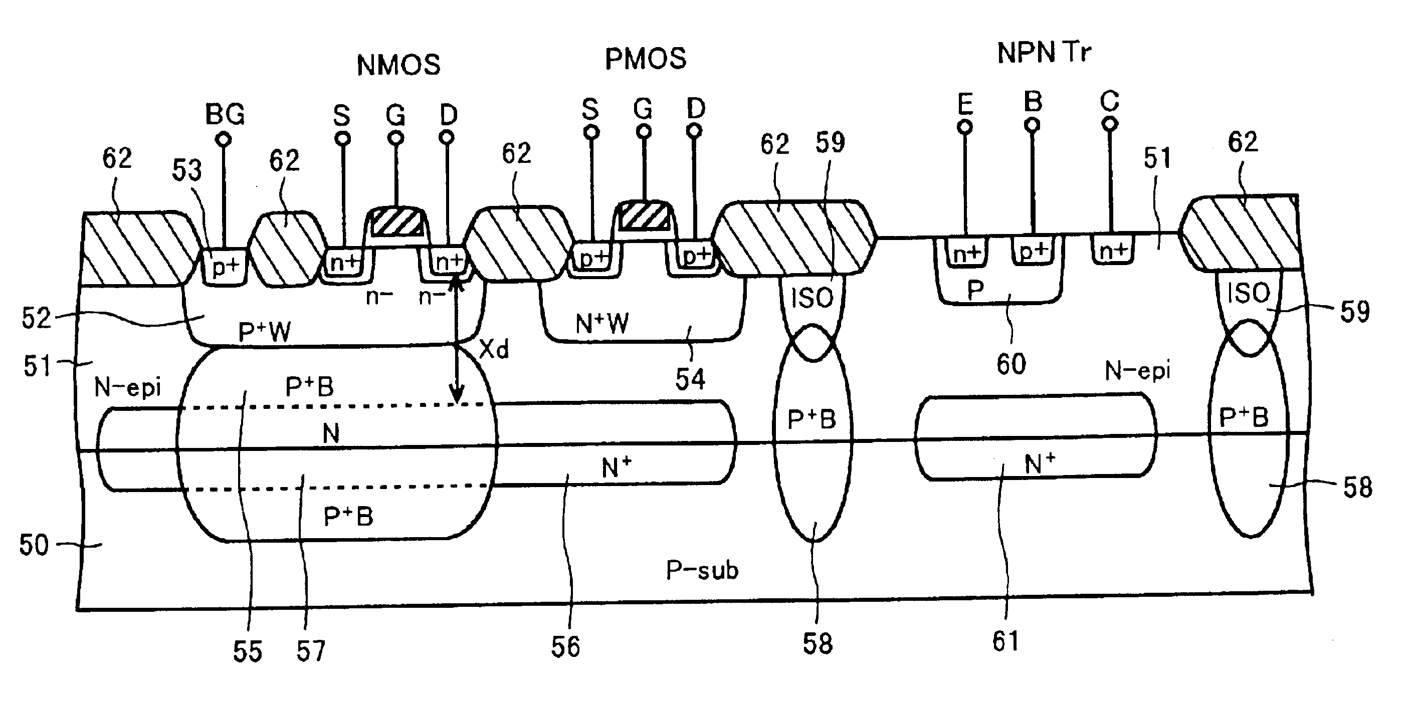
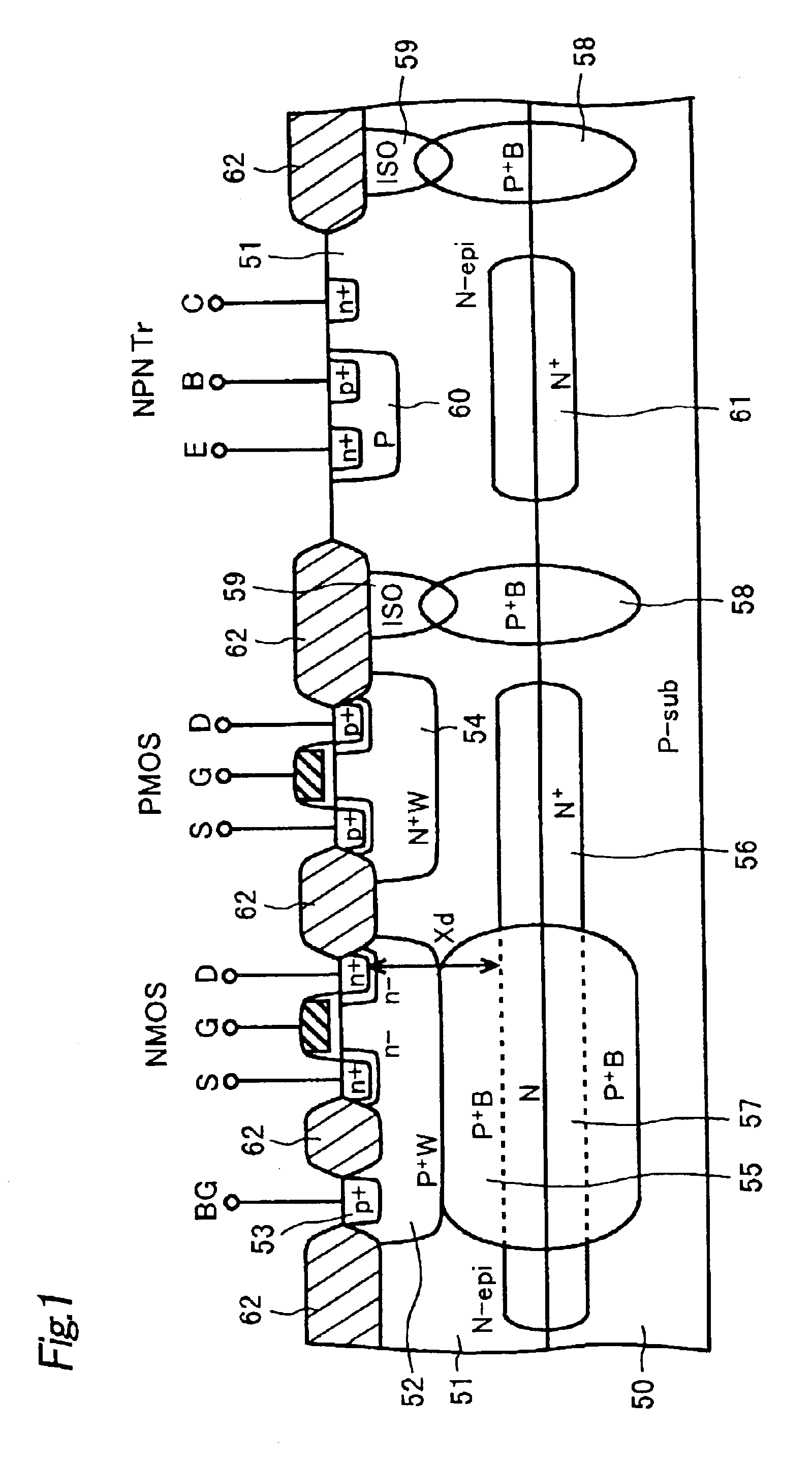
FIG. 5 is a cross-sectional view showing a charge pump device according to this invention.

Circuit structure of this charge pump device is similar to that of the first embodiment. The charge transfer MOS transistors M2 and M3 of the charge pump device of FIG. 19 are shown in FIG. 5, as in the case of the first embodiment.

Difference from the first embodiment is that the P+-type buried layer 55 is not formed below the P-type well regions 52A and 52B. Although the effect to reduce the resistance of the P-type well regions 52A and 52B is lost because of the lack of the P+-type buried layer 55, it seems that robustness against latch up is increased compared with the conventional charge pump device by adding the lower isolation layer 58 and the upper isolation layer 59.

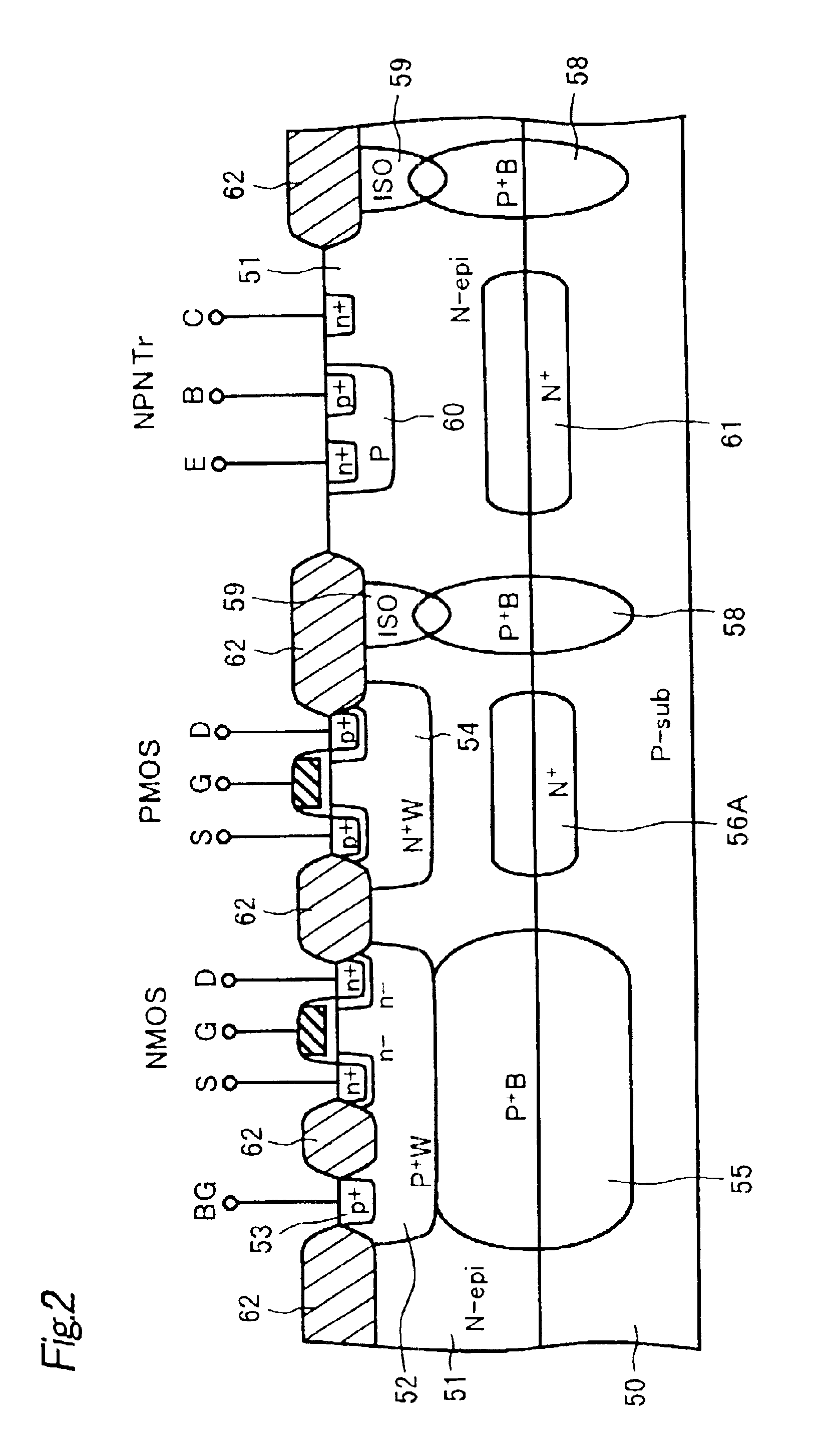
FIG. 6 is a cross-sectional view showing a charge pump device according to a third embodiment of this invention. Circuit structure of this charge pump device is similar to that of the first embodiment. The charge transfer MO...


PUM


Abstract

A latch up in a charge pump device is prevented as well as a withstand voltage of an MOS transistor used in the charge pump device is increased with this invention. A first and a second N-type epitaxial silicon layers are stacked on a P-type single crystalline silicon substrate, and P-type well regions are formed in the second epitaxial silicon layer separated from each other. A P-type isolation layer is formed between the P-type well regions. A P+-type buried layer is formed abutting on a bottom of each of the well regions, an N+-type buried layer is formed abutting on a bottom of the P+-type buried layer, and a transistor for charge transfer is formed in each of the P-type well regions.

Description

BACKGROUND OF THE INVENTION1. Field of the InventionThis invention relates to a charge pump device with large current capacity used for a power supply circuit and the like, specifically to a charge pump device enabled stable operation by preventing a latch up.2. Description of the Related ArtVideo equipment in recent years such as a camcorder, a digital still camera (DSC) and a mobile phone with DSC use CCDs (charge-coupled devices) to capture an image. A CCD drive circuit for driving the CCDs requires a power supply circuit that provides both positive and negative high voltages (over 10 volts) and a large current (several milliamperes). A switching regulator is used for that purpose today.The switching regulator can generate a high voltage with high performance, i.e. with high power efficiency (output power / input power). However, it has a drawback to generate a harmonic noise when switching a current. Therefore, the power supply has to be used with a noise shield. In addition to th...

Claims


Application Information

Patent Timeline
Patent Type & Authority Patents(United States)
IPC IPC(8): H01L27/02H01L27/06H02M3/04H02M3/07H01L21/822H01L27/04H01L21/8249
CPCH01L27/0218H02M3/073H01L27/0623G05F1/10
Inventor KANEKO, SATORUOHKODA, TOSHIYUKIMYONO, TAKAO
Owner SEMICON COMPONENTS IND LLC
Why Eureka
Try Eureka