Solution-processed thin film transistor formation method

a technology of thin film transistors and formation methods, which is applied in the direction of semiconductor devices, solid-state devices, electrical apparatuses, etc., can solve the problems of increasing complexity and expense, reducing the efficiency of the device, so as to achieve the effect of simply manufacturing devices and circuits

Inactive Publication Date: 2005-03-15
HEWLETT PACKARD DEV CO LP
View PDF8 Cites 39 Cited by
  • Summary
  • Abstract
  • Description
  • Claims
  • Application Information

AI Technical Summary

Problems solved by technology

A critical issue, however, remains feature size.
However, introducing conventional techniques to produce small feature sizes, e.g., lithography, adds complexity and expense that contradicts the goal of achieving simply manufactured devices and circuits.
Solution-processed deposition also places demands on the materials used to form features, particularly when an ink jet deposition process is utilized.
Other techniques may produce smaller sized gaps, but have limitations such as being limited to use on small substrates.

Method used


Image

  • Solution-processed thin film transistor formation method
  • Solution-processed thin film transistor formation method
  • Solution-processed thin film transistor formation method

Examples


Embodiment Construction

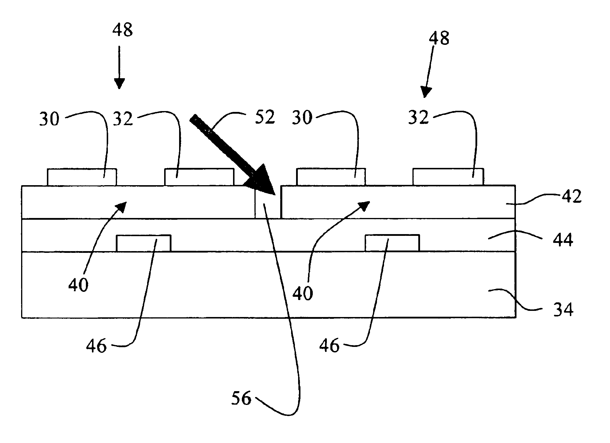
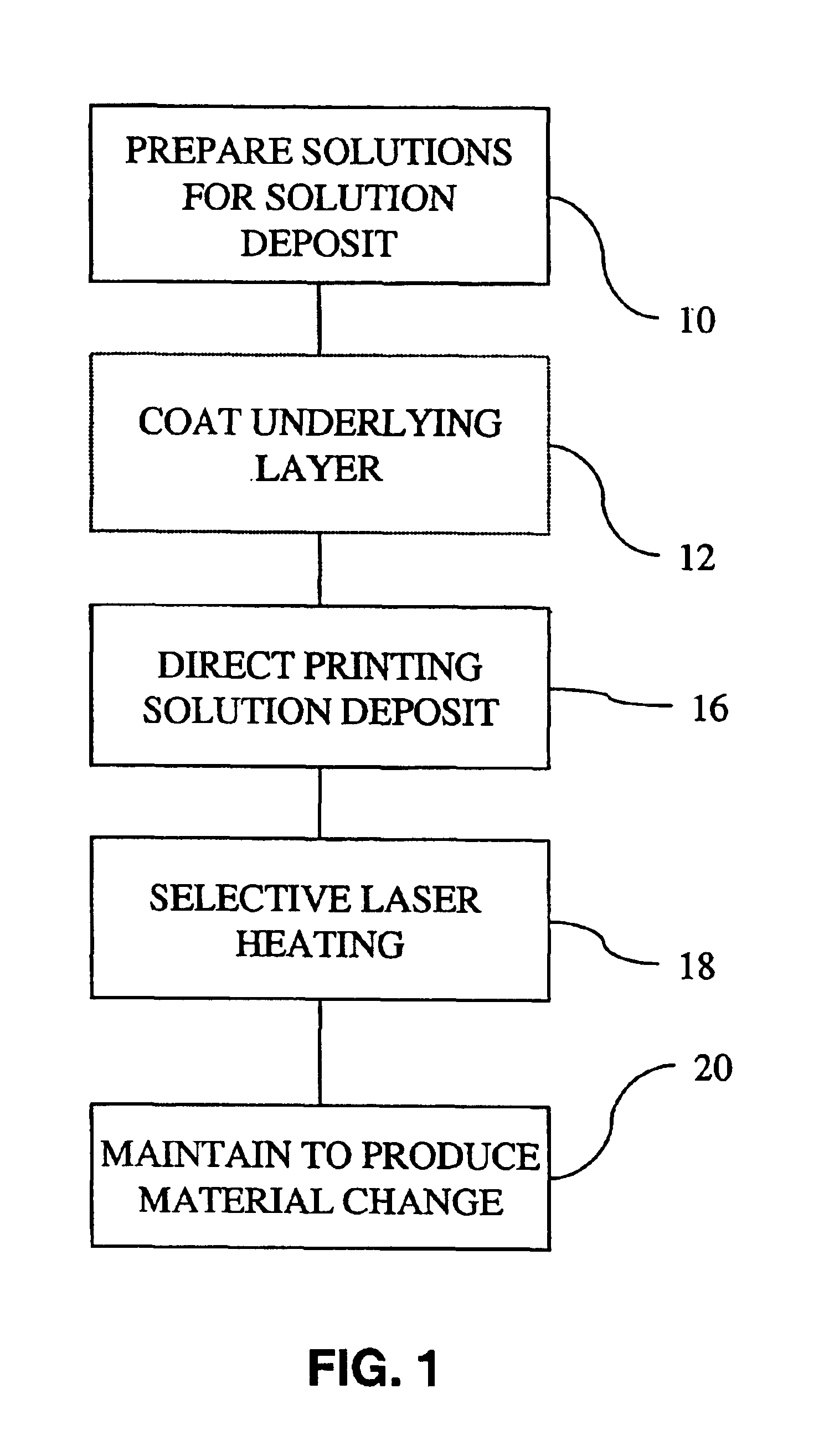
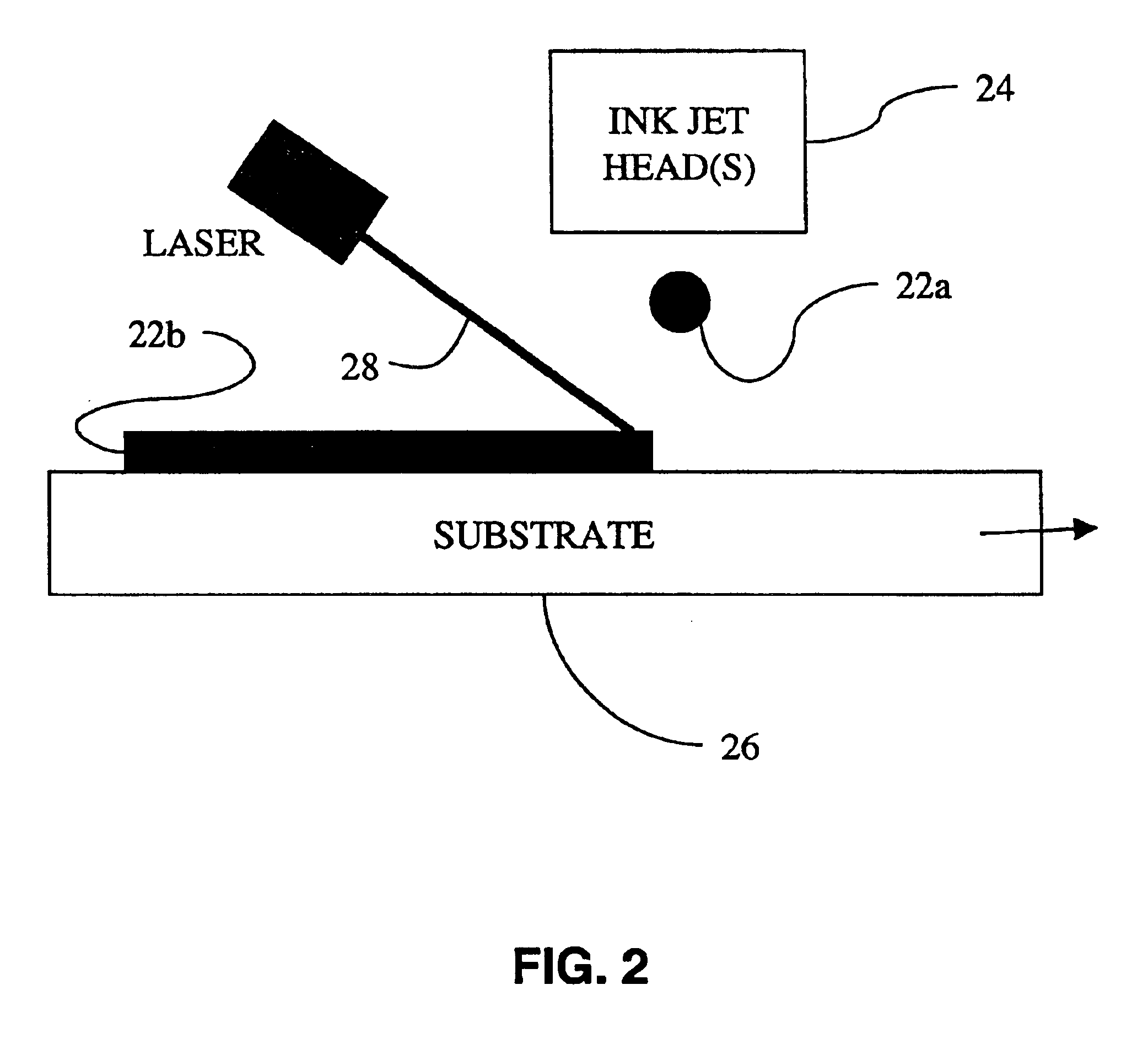
The invention concerns solution-processed thin film transistor formation that makes use of selective laser heating to affect a solution phase deposited semiconductor material. An exemplary solution-processed thin film transistor formation method of the invention forms solution-processed thin film layers into a transistor structure. During formation, semiconductor portions of the transistor structure are selectively heated via a laser to modify the material state of semiconductor material from a solution deposited material state to a thin film layer material state.

In exemplary embodiments, the laser heating vaporizes solvent to leave a semiconductor material that was part of the solution. At the same time, the semiconductor material released from the solvent is cured, annealed, sintered or recrystallized depending upon the particular semiconductor material being deposited. In exemplary embodiments, ablation is also employed to remove material as part of a patterning step for the semi...


PUM

PropertyMeasurementUnit
wavelengthsaaaaaaaaaa
dissolvingaaaaaaaaaa
conductiveaaaaaaaaaa

Abstract

An exemplary solution-processed thin film transistor formation method of the invention forms solution-processed thin film layers into a transistor structure. During formation, semiconductor portions of the transistor structure are selectively heated via a laser to modify the material state of semiconductor material from a solution deposited material state to a thin film layer material state.

Description

FIELD OF THE INVENTIONThe invention is in the semiconductor field. The invention particularly concerns solution-processed thin film transistors.BACKGROUND OF THE INVENTIONSolution-processed thin film transistors hold great promise to fundamentally change the semiconductor industry. Their uses run the gamut of conventional transistor uses, and may be formed into light emitting structures. Materials used in the thin films, such as conductive polymers, are durable and can be flexible, thereby providing a range of uses in demanding environments.The solution-processed thin film transistors also hold the potential to be fabricated by simple techniques, e.g., direct printing of circuits. A long-term goal is to have circuits of solution-processed thin film transistors printed on a substrate in similar fashion to the way ink is patterned in a printing press. Proposed manufacturing techniques seek to employ relatively simple procedures such as inkjet printing. A critical issue, however, remai...

Claims


Application Information

Patent Timeline
Patent Type & Authority Patents(United States)
IPC IPC(8): H01L51/40H01L51/05H01L51/30H01L51/00
CPCH01L51/0004H01L51/0021H01L27/283H01L51/0545H01L51/0037H01L51/0516H01L51/0541H01L51/0036H10K19/10H10K71/13H10K71/60H10K85/1135H10K85/113H10K10/468H10K10/464H10K10/466
Inventor WENG, JIAN-GANGKWASNY, DAVID M.ORR, DAVID
Owner HEWLETT PACKARD DEV CO LP
Why Eureka
Try Eureka