

Method for electrochemically processing a workpiece
a workpiece and workpiece technology, applied in the direction of basic electric elements, electrical equipment, semiconductor devices, etc., can solve the problems of high pressure used in the cmp process, affecting the mechanical strength of silicon oxide, and affecting the efficiency of the cmp process
- Summary
- Abstract
- Description
- Claims
- Application Information
AI Technical Summary
Benefits of technology
Problems solved by technology
Method used
Image

Examples
Embodiment Construction
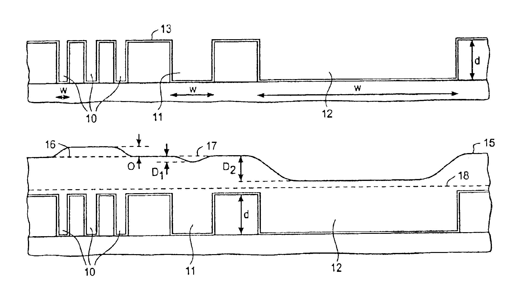
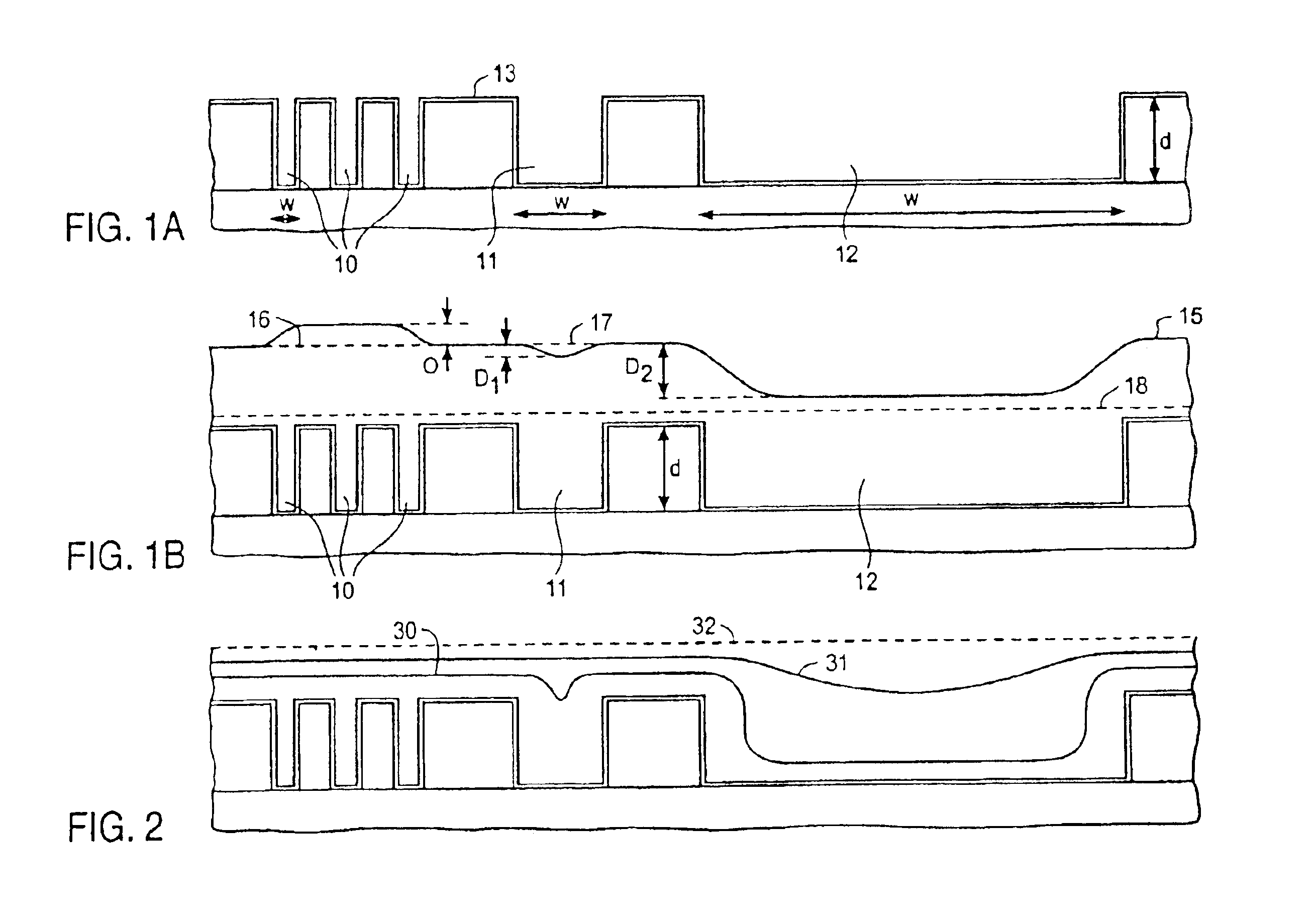
The process of the present invention relates to a process for forming a near-planar or planar layer of a conducting material, such as copper, on a surface of a workpiece using an ECMPR technique such as ECMD. The process of the present invention preferably uses at least two separate plating solution chemistries to form a near-planar or planar copper layer on a semiconductor substrate that has features or cavities on its surface. The unique feature of the present invention is the fact that it can be applied to substrates with features or cavities of a wide variety shapes and dimensions. For example, the substrate may have high-aspect ratio small size features, such as sub-micron size vias or trenches, as well as very low aspect-ratio features such as larger than 10 micron wide trenches and larger than 20 micron size pads or channels. There may even be larger than 500 micron features on this exemplary wafer. At a first stage of the present invention, a plating process that is optimize...
PUM
| Property | Measurement | Unit |
|---|---|---|
| Time | aaaaa | aaaaa |
| Acceleration | aaaaa | aaaaa |
| Electrical conductor | aaaaa | aaaaa |
Abstract
Description
Claims
Application Information