Method of chemical/mechanical polishing of the surface of semiconductor device

a technology of chemical/mechanical polishing and semiconductor devices, applied in the direction of polishing compositions, lapping machines, manufacturing tools, etc., can solve the problem of difficult deformation of polishing pads, and achieve the effect of keeping scratches from increasing

Inactive Publication Date: 2005-03-15
KK TOSHIBA
View PDF18 Cites 5 Cited by
  • Summary
  • Abstract
  • Description
  • Claims
  • Application Information

AI Technical Summary

Benefits of technology

It is therefore an object of the present invention to provide a semiconductor device chemical/mechanical

Problems solved by technology

According to the chemical/mechanical polishing methods, since the to-be-polished surface of the semiconductor device is polished

Method used


Image

  • Method of chemical/mechanical polishing of the surface of semiconductor device
  • Method of chemical/mechanical polishing of the surface of semiconductor device
  • Method of chemical/mechanical polishing of the surface of semiconductor device

Examples


Embodiment Construction

An embodiment of the present invention will be described hereinafter with reference to the accompanying drawings, wherein like reference characters designate like parts throughout all the views.

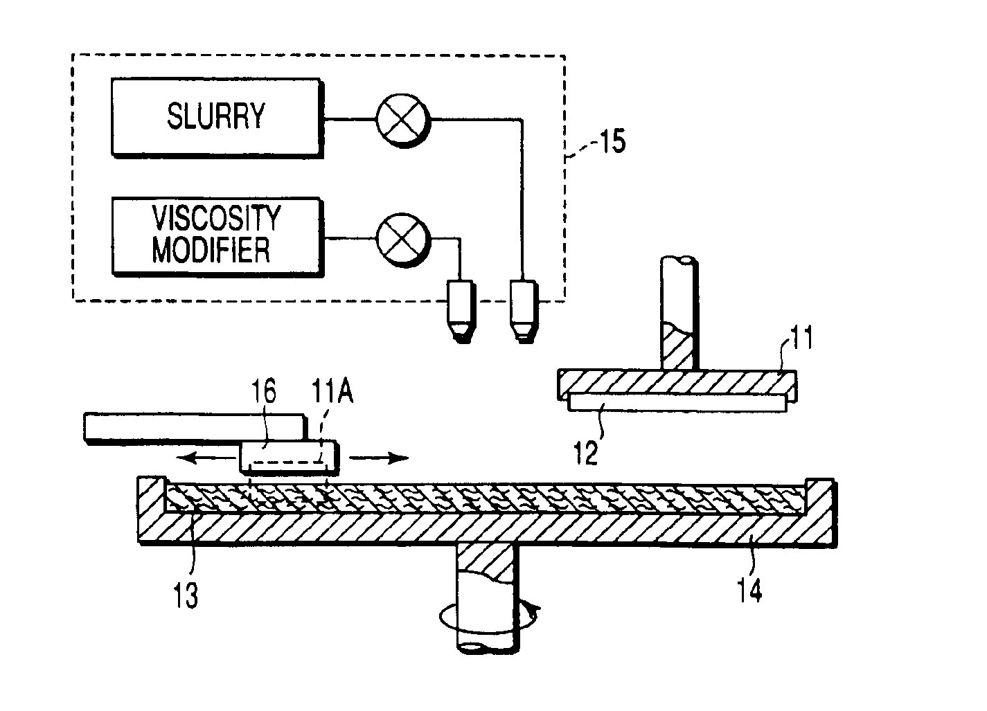
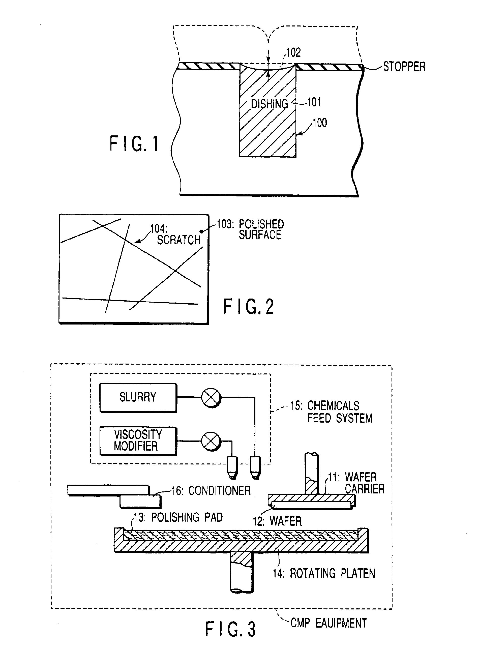
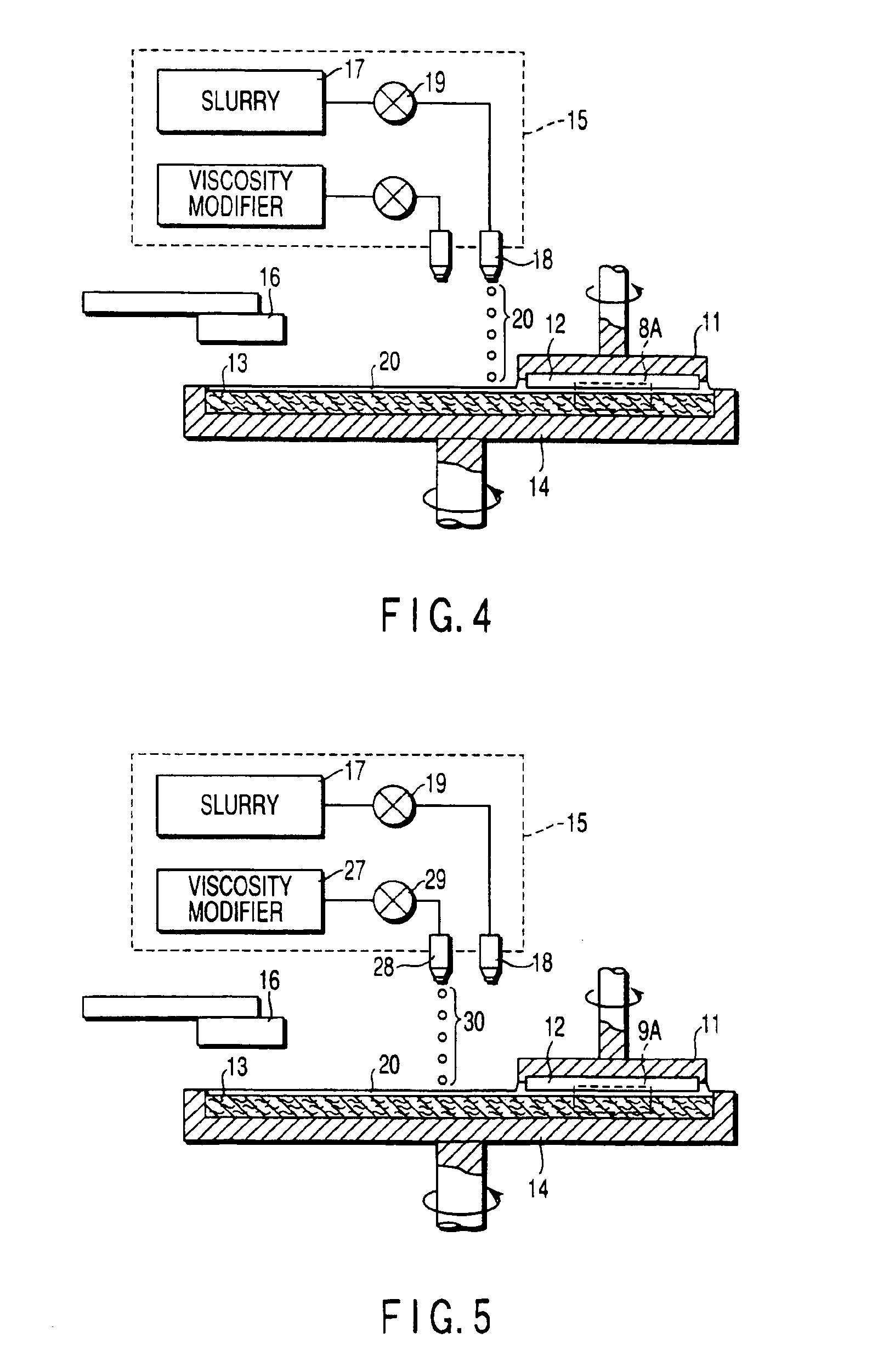
First, reference is made to FIG. 3 to describe CMP equipment used in the CMP process according to an embodiment of the present invention.

As shown in FIG. 3, a wafer carrier 11 holds a wafer 12. The wafer 12 is held by the carrier 11 so that its to-be-polished surface is opposed to a polishing pad 13. The polishing pad 13 is mounted on a rotating platen 14. In this embodiment, the polishing pad 13 may be a conventionally used one. For example, the polishing pad 13 is preferably formed of a foam material consisting of, say, polyurethane, non-woven fabric consisting of, say, polyester fiber, or a stacked structure of these materials.

Above the rotating platen 14 is provided a chemicals feed system 15 which feeds the polishing pad 13 with chemicals. In this embodiment, the chemicals comprise a slu...


PUM

PropertyMeasurementUnit
Surface activityaaaaaaaaaa

Abstract

The surface of a semiconductor device is polished by first supplying a polishing pad with a slurry that contains a solvent, abrasive grains, and an additive for making the viscosity of the slurry variable so that the top portion of the polishing pad is soaked with the slurry, then supplying the polishing pad with a viscosity modifier for increasing the viscosity of the slurry and hardening the top portion of the polishing pad soaked with the slurry, and finally polishing the surface of the semiconductor device with the slurry having its viscosity increased and the polishing pad having its top portion hardened.

Description

BACKGROUND OF THE INVENTIONThe present invention generally relates to a method of manufacturing a semiconductor device and more particularly to methods of chemical / mechanical polishing of the surface of a semiconductor device.The chemical / mechanical polishing (CMP) has been used for planarization of interlayer insulating films, metal interconnections, polysilicon filling device isolation trenches, etc.In planarizing polysilicon by CMP, a stopper film consisting of silicon dioxide or nitride silicon is used in order to stop the progress of polishing after planarization. In this case, it is required to polish polysilicon selectively in comparison with the stopper film.In the CMP, however, polishing / etching is performed based on the combined action of the chemical action of a polishing slurry and the mechanical action of abrasive grains. Depending on selected polishing conditions, therefore, “dishing” may occur. The “dishing” means that a recess 102 is formed, as shown in FIG. 1, on to...

Claims


Application Information

Patent Timeline
IPC IPC(8): B24B37/04C09G1/00C09G1/02H01L21/02H01L21/321H01L21/304
CPCB24B37/044H01L21/3212C09G1/02H01L21/304
Inventor MIYASHITA, NAOTONISHIOKA, TAKESHI
Owner KK TOSHIBA
Why Eureka
Try Eureka