Flash-preventing semiconductor package

a technology of semiconductor packaging and flash prevention, which is applied in the direction of semiconductor devices, semiconductor/solid-state device details, electrical equipment, etc., can solve the problems of structural cracks or electricity loss, increase the viscosity and cost of underfilling materials, and material filling is often too slow, so as to reduce the flow speed, reduce the cost of underfilling materials, and absorb heat rapid

Inactive Publication Date: 2005-03-15
SILICONWARE PRECISION IND CO LTD
View PDF18 Cites 20 Cited by
  • Summary
  • Abstract
  • Description
  • Claims
  • Application Information

AI Technical Summary

Benefits of technology

A primary objective of the present invention is to provide a semiconductor package and a method for fabricating the same, in which flash of an encapsulating material can be prevented from occurring around air vents, so that the quality and appearance of the semiconductor package can be well maintained.
Another objective of the invention is to provide a semiconductor package and a method for fabricating the same, in which a molded underfilling technology is employed, and an encapsulating material having low viscosity and fine fillers can be used as to reduce the underfilling time.
A further objective of the invention is to provide a semiconductor package and a method for fabricating the same, in which an encapsulating material having low viscosity and fine fillers can be used to prevent flash thereof from occurring in a molded underfilled BGA semiconductor package with a highly integrated chip.
Due to the recess portions relatively smaller in height, the molding compound more rapidly absorbs heat transmitted from the mold and thus slows down its flow when flowing into the recess portions of the molding cavity The slowed down molding compound with increased viscosity can therefore be prevented from flashing out of the air vents, so that quality and appearance of the fabricated semiconductor package can be well assured.

Problems solved by technology

If this undercavity is not filled with an insulative material, due to the difference in coefficient of thermal expansion (CTE) between the chip and the substrate, during a temperature cycle in subsequent processes, the chip and the substrate respectively suffer different thermal stress, thereby easily resulting in structural cracks or electricity loss.
However, this technology has the following drawbacks.
First, it is time-consuming.
In such a flip chip underfilling process, the insulative material is filled in a capillary filling manner around the chip; thus, the material filling is often too slow with voids easily being formed.
However, the addition of the solid filler greatly increases the viscosity and cost of the underfilling material.
However, due to the encapsulating material 19 having low viscosity (high fluidity) and fine fillers, it often unavoidably flashes around the air vents 17 after completing the molding process, as shown in FIG.
This therefore seriously deteriorates the quality and appearance of the FCBGA semiconductor package 1.
However, the flash problem still can not be eliminated when the encapsulating material flows through a plurality of air vents located at corners, as shown in the drawing.

Method used


Image

  • Flash-preventing semiconductor package
  • Flash-preventing semiconductor package
  • Flash-preventing semiconductor package

Examples


Embodiment Construction

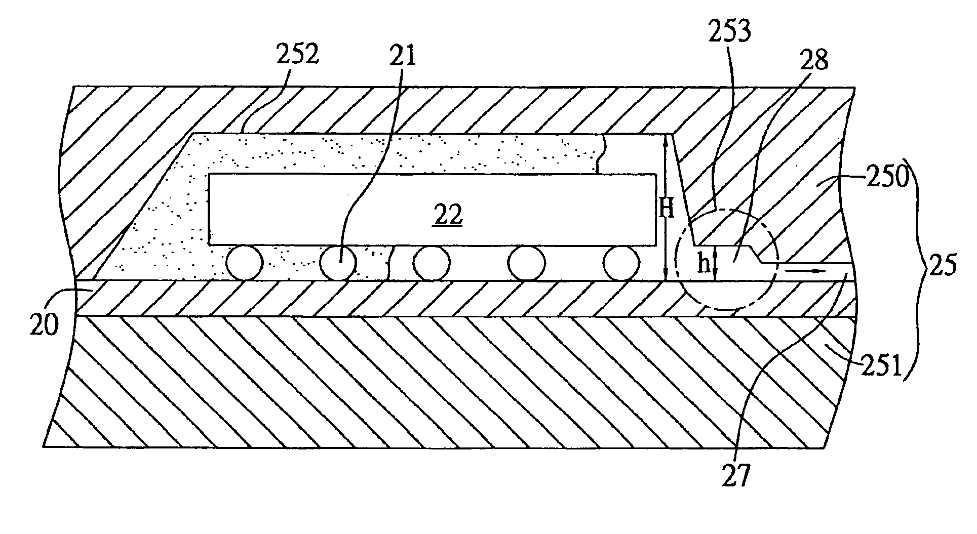
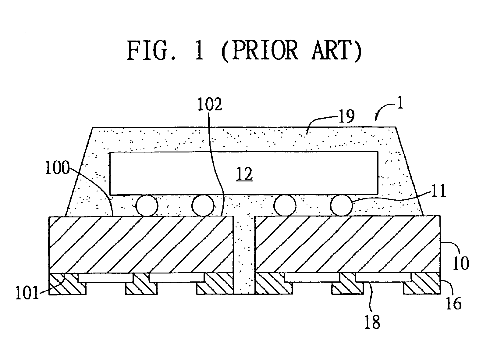
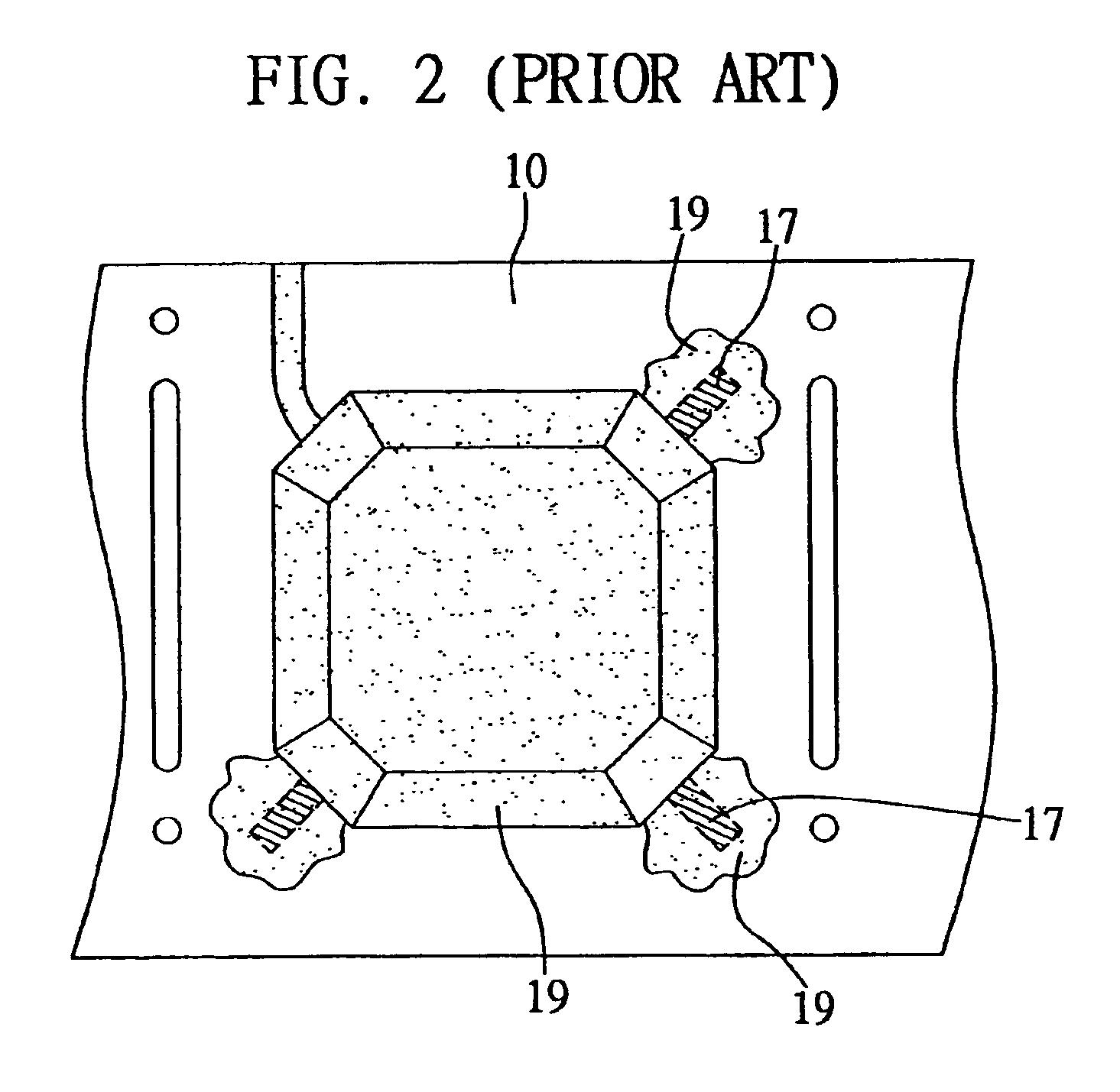
A semiconductor package and a method for fabricating a semiconductor package proposed in the present invention are fully described in the following embodiments with reference to FIGS. 3-7, wherein the method is applicable for fabricating all types of BGA (ball grid array) semiconductor packages, and a FCBGA (flip chip ball grid array) semiconductor package is exemplified herein, in an effort to depict a molded underfilling technology in detail.

FIGS. 3A and 3B illustrate a top view and a sectional view of a BGA semiconductor package 2 of the invention, respectively. As shown in the drawings, the BGA semiconductor package 2 comprises a substrate 20; a semiconductor chip 22 reflowed on the substrate 20 by a plurality of solder bumps 21; a plurality of solder balls 23 implanted on a back surface 201 of the substrate 20 for electrically connecting the semiconductor chip 22 to external devices; and an encapsulant 29 for encapsulating the semiconductor chip 22, and formed with a plurality ...


PUM


Abstract

A semiconductor package and a method for fabricating the same are proposed, wherein, in a molding process for encapsulating a semiconductor chip mounted on a substrate, a mold is used with a molding cavity formed with a plurality of recess portions relatively smaller in height, and with a plurality of air vents for connecting the recess portions to outside of the mold and for ventilate air in the molding cavity. This allows a molding resin used during molding to slow down its flow when flowing into the recess portions, as the molding resin rapidly absorbs heat transmitted from the mold and is increased in viscosity thereof. The slowed down molding resin can therefore be prevented from flashing out of the air vents, so that quality and appearance of the fabricated semiconductor package can be well assured.

Description

FIELD OF THE INVENTIONThe present invention relates to semiconductor packages and methods for fabricating the same, and more particularly, to a semiconductor package and a method for fabricating the same, in which resin flash can be prevented from occurrence in a BGA (ball grid array) semiconductor package.BACKGROUND OF THE INVENTIONA ball grid array (BGA) semiconductor package employs advanced semiconductor packaging technology, in which a substrate has a front side for mounting a semiconductor chip thereon and a back side for disposing a plurality of solder balls thereon, so as to provide high density of I / O connections, and to bond and electrically connect the semiconductor package to an external printed circuit board.A flip chip ball grid array (FCBGA) semiconductor package is an improved BGA semiconductor package, wherein the semiconductor chip is bonded in an upside down manner to the front side of the substrate via a plurality of solder bumps, and is electrically connected to...

Claims


Application Information

Patent Timeline
Patent Type & Authority Patents(United States)
IPC IPC(8): H01L21/56H01L21/02
CPCH01L21/565H01L2224/73265H01L2924/1815H01L2224/32225H01L2924/15311H01L2224/16225H01L2224/45144H01L2924/00014H01L2924/00H01L2224/0401
Inventor HUANG, CHIEN-PINGHO, TZONG-DA
Owner SILICONWARE PRECISION IND CO LTD
Why Eureka
Try Eureka