Silicide proximity structures for CMOS device performance improvements

a proximity structure and semiconductor technology, applied in the direction of semiconductor devices, electrical equipment, transistors, etc., can solve the problems of higher cost, disadvantageous to the performance of pfet, and beneficial to the performance of an n

Inactive Publication Date: 2005-03-22
GLOBALFOUNDRIES INC
View PDF69 Cites 56 Cited by
  • Summary
  • Abstract
  • Description
  • Claims
  • Application Information

AI Technical Summary

Problems solved by technology

However, the same stress component, either tensile stress or compressive stress, discriminatively affects the characteristics of an n-type device and a p-type device.
That is, because the type of stress which is beneficial for the performance of an NFET is generally disadvantageous for the performance of the PFET.
While these methods do provide structures that have tensile stresses being applied to the NFET device and compressive stresses being applied along the longitudinal direction of the PFET device, they may require additional materials and / or more complex processing, and thus, resulting in higher cost.

Method used


Image

  • Silicide proximity structures for CMOS device performance improvements
  • Silicide proximity structures for CMOS device performance improvements
  • Silicide proximity structures for CMOS device performance improvements

Examples


Embodiment Construction

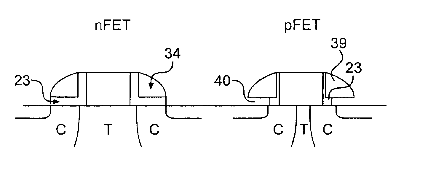
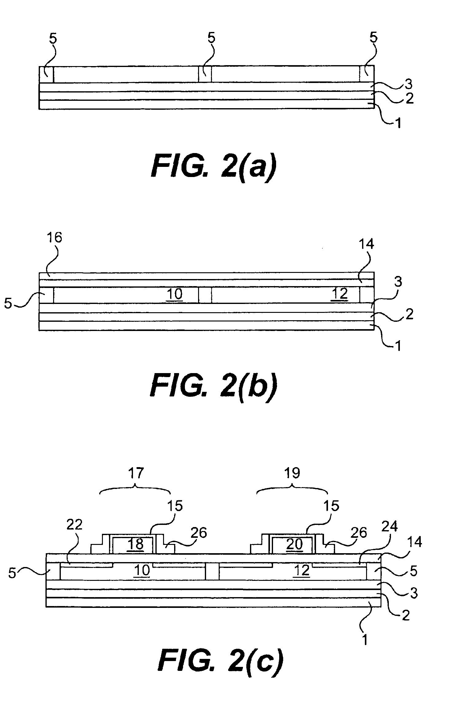
The invention provides a method for fabricating devices with improved performance characteristics. The invention relates to the improved characteristics of a device. Generally, silicidation is known to create significant stresses in the silicon and that stress distributions resulting from silicidation are highly nonuniform. These properties of silicidation are used by the invention to control the stresses in complimentary metal oxide semiconductor (CMOS)PFETs and NFETs. In an embodiment of the invention, different spacer widths and undercut combinations are used to modulate silicide distances in order to control the stress in the channels of NFET and PFET devices.

In the methods and devices according to the invention, the stresses are self-aligned to the gate. In the devices formed with the isolation induced stress structures, the stresses are not self-aligned to the gate. In addition, in the methods and devices according to the invention, the stress levels attained under the gate in...


PUM


Abstract

A method for manufacturing an integrated circuit having a plurality of semiconductor devices including an n-type field effect transistor and a p-type field effect transistor on a semiconductor wafer by creating a spacer having a first width for the n-type field effect transistor and creating a spacer having a second width for the p-type field effect transistor, the first width being greater than the second width and depositing silicide material on the semiconductor wafer such that tensile mechanical stresses are formed within a channel of the n-type field effect transistor and compressive stresses are formed within a channel of the p-type field effect transistor.

Description

BACKGROUND OF INVENTIONThe invention generally relates to methods for manufacturing a semiconductor device with improved device performance, and more particularly to methods for manufacturing semiconductor devices which impose tensile and compressive stresses in the substrate of the device during device fabrication.Mechanical stresses within a semiconductor device substrate can modulate device performance. That is, stresses within a semiconductor device are known to enhance semiconductor device characteristics. Thus, to improve the characteristics of a semiconductor device, tensile and / or compressive stresses are created in the channel of the n-type devices (e.g., NFETs) and / or p-type devices (e.g., PFETs). However, the same stress component, either tensile stress or compressive stress, discriminatively affects the characteristics of an n-type device and a p-type device.In order to maximize the performance of both NFETs and PFETs within integrated circuit (IC) chips, the stress comp...

Claims


Application Information

Patent Timeline
Patent Type & Authority Patents(United States)
IPC IPC(8): H01L21/38H01L21/02H01L21/28H01L21/336H01L21/8238H01L21/84H01L27/12H01L29/45H01L29/786
CPCH01L21/823807H01L21/823864H01L21/84H01L27/1203H01L29/78654H01L29/66772H01L29/7842H01L29/7845H01L29/458
Inventor CHIDAMBARRAO, DURESETIDOKUMACI, OMER H.RENGARAJAN, RAJESHSTEEGEN, AN L.
Owner GLOBALFOUNDRIES INC
Why Eureka
Try Eureka