Semiconductor imaging sensor array devices with dual-port digital readout

Inactive Publication Date: 2005-03-22
APTINA IMAGING CORP
View PDF9 Cites 57 Cited by
  • Summary
  • Abstract
  • Description
  • Claims
  • Application Information

AI Technical Summary

Benefits of technology

The first and second memory cells are coupled to read a first digital pixel signal generated from a first sensing pixel into one of said first and second memory cells while the other memory cell outputs a second digital pixel signal that i

Problems solved by technology

The digital readout of the imaging sensors may be delayed by the limited bandwidth and limited transfer sp

Method used


Image

  • Semiconductor imaging sensor array devices with dual-port digital readout
  • Semiconductor imaging sensor array devices with dual-port digital readout
  • Semiconductor imaging sensor array devices with dual-port digital readout

Examples


Example

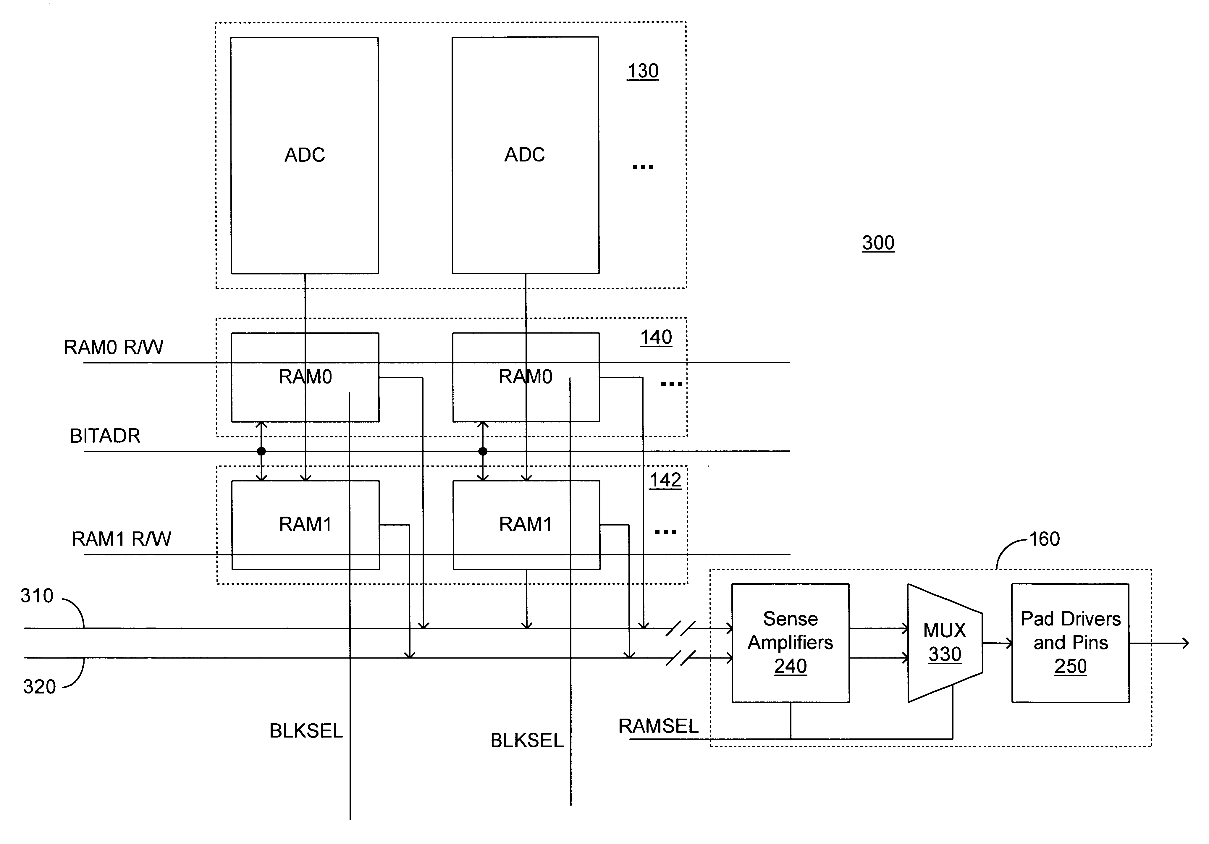
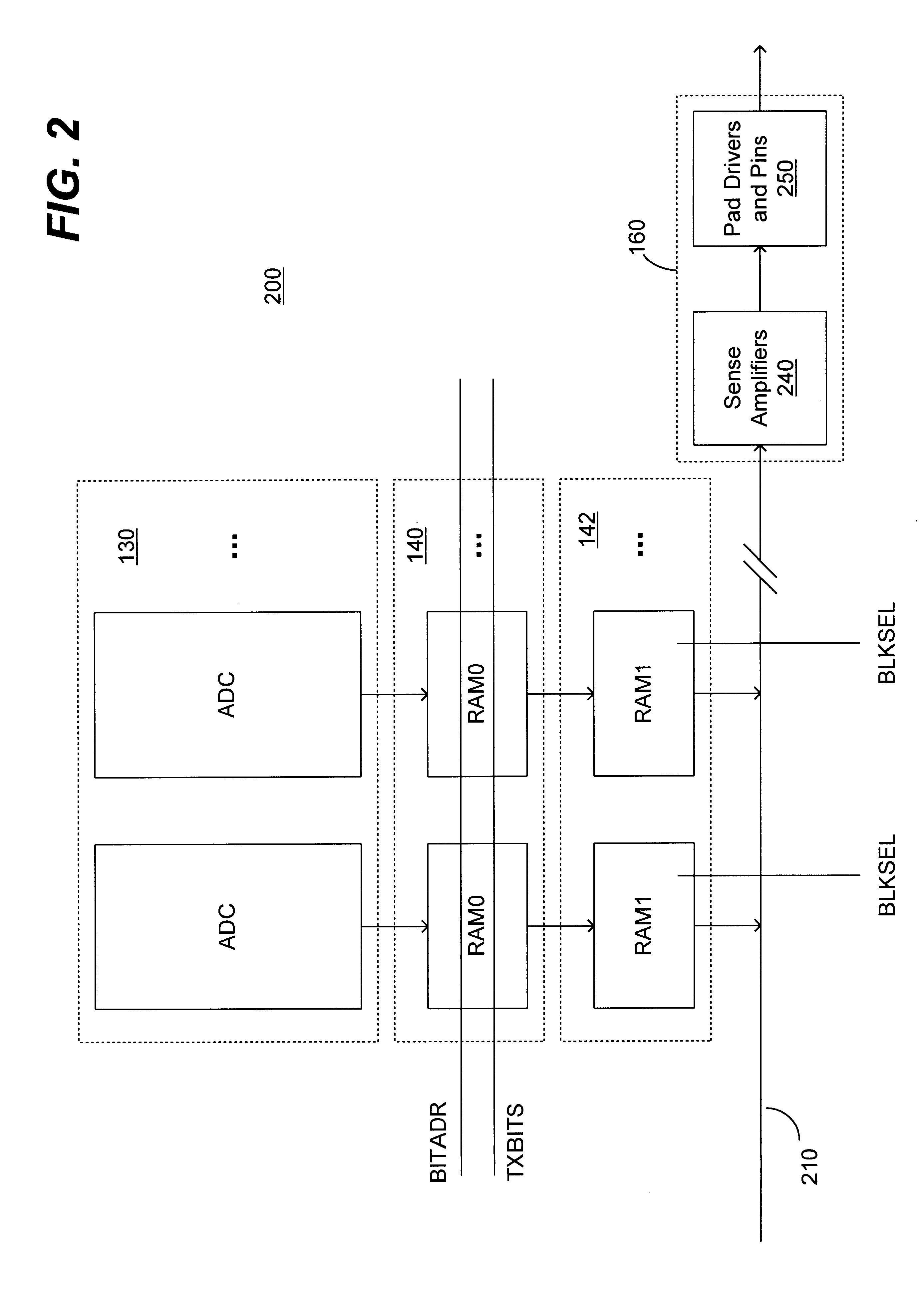
A semiconductor imaging device may integrate an imaging sensor array of multiple sensing pixels, and certain controlling and processing circuits on a single semiconductor substrate. Analog-to-digital conversion function may also be integrated by forming one or more ADCs on the same substrate where the sensing pixels are located. Such integrated imaging devices with on-chip ADCs can be used to reduce the size, power consumption, and manufacturing cost. Such ADC integration can also improve the device reliability, noise immunity (e.g., cross talk, clock pickup, electromagnetic interference), and chip-to-chip interfacing (e.g., from the sensor to a computer).

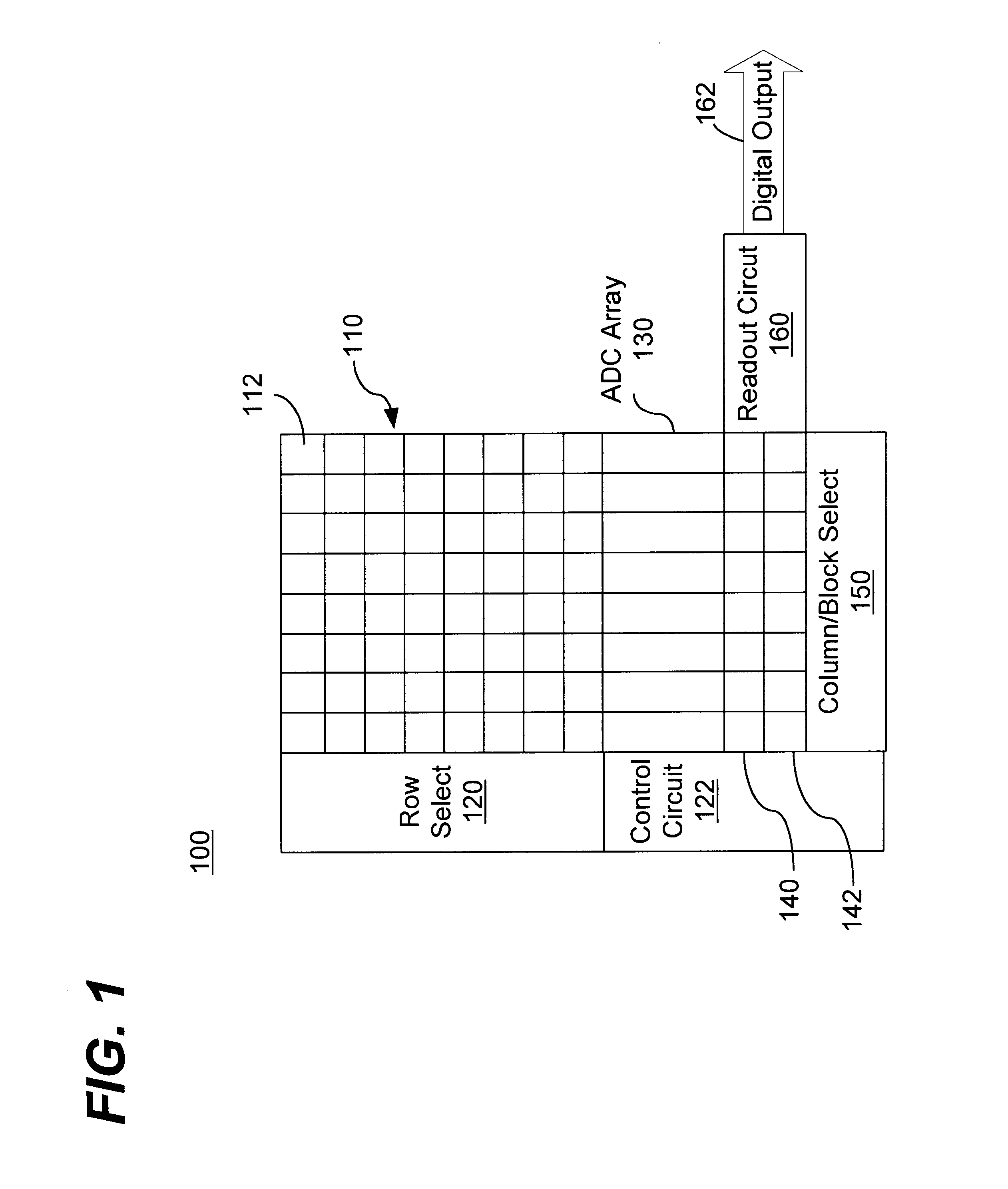
FIG. 1 shows an embodiment of a semiconductor imaging device 100 with on-chip ADCs. A sensor array 110 includes an array of sensing pixels 112 in rows and columns fabricated over a semiconductor substrate. Each sensing pixel includes a semiconductor photosensor to convert received radiation into an electrical signal (e.g., electric...


PUM


Abstract

Imaging sensors having dual-port for digital readout to pipeline readout processes of two different groups of pixels.

Description

BACKGROUNDThis disclosure is related to semiconductor imaging devices and techniques, and more specifically, to semiconductor imaging arrays with integrated analog-to-digital converters.A typical semiconductor imaging sensor includes a pixel array of photosensors and associated controlling and processing circuits. An optical image captured by the imaging sensor is first converted into analog electrical signals and then processed by the processing circuits in either analog mode or digital mode. In the digital mode, one or more analog-to-digital converters (“ADCs”) may be used to convert the analog signals into a digital representation of the image.The digital readout of the imaging sensors may be delayed by the limited bandwidth and limited transfer speed of the readout bus. Such readout delay can be particularly prominent when the number of pixels is large.SUMMARYThe present semiconductor imaging devices include readout devices and techniques based on a dual-port configuration in wh...

Claims


Application Information

Patent Timeline
IPC IPC(8): H04N3/15H04N5/357H04N5/369
CPCH04N5/335H04N3/1575H04N25/00H04N25/75
Inventor BLERKOM, DANIEL VANKRYMSKI, ALEXANDERKOTLYAR, ABEBOCK, NIKOLAIANDERSSON, ANDERSMANSOORIAN, BARMAK
Owner APTINA IMAGING CORP
Why Eureka
Try Eureka