Coaxial narrow angle dark field lighting

a narrow angle, dark field technology, applied in the field of imaging optics, can solve the problems of degraded image, small angle, premature device failure,

Inactive Publication Date: 2005-03-22
ELECTRO SCI IND INC
View PDF11 Cites 58 Cited by
  • Summary
  • Abstract
  • Description
  • Claims
  • Application Information

AI Technical Summary

Problems solved by technology

After the devices have been singulated (generally cut by saw into individual rectangular devices), it may be necessary to inspect the edges for small chips and cracks that may propagate over time and cause premature device failure.
If the object is specular, that is if the objec...

Method used


Image

  • Coaxial narrow angle dark field lighting
  • Coaxial narrow angle dark field lighting
  • Coaxial narrow angle dark field lighting

Examples


Embodiment Construction

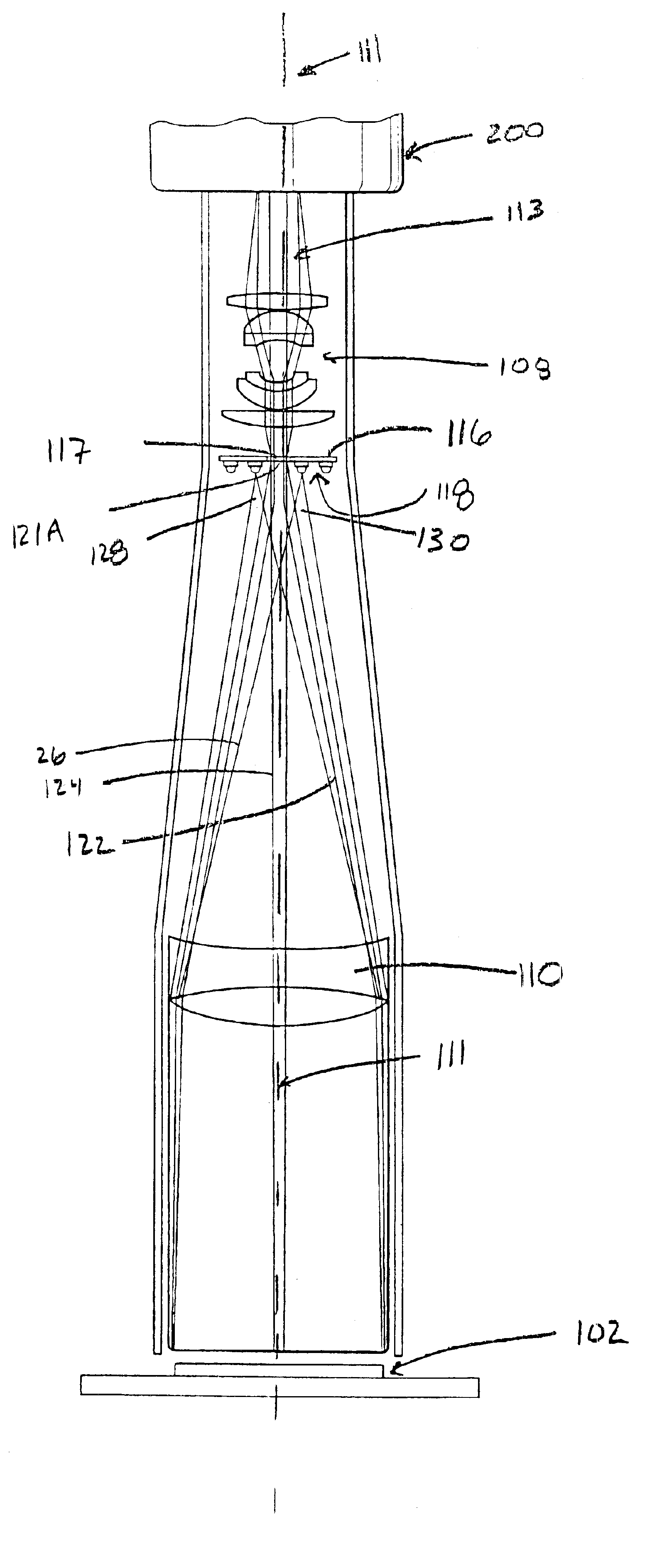
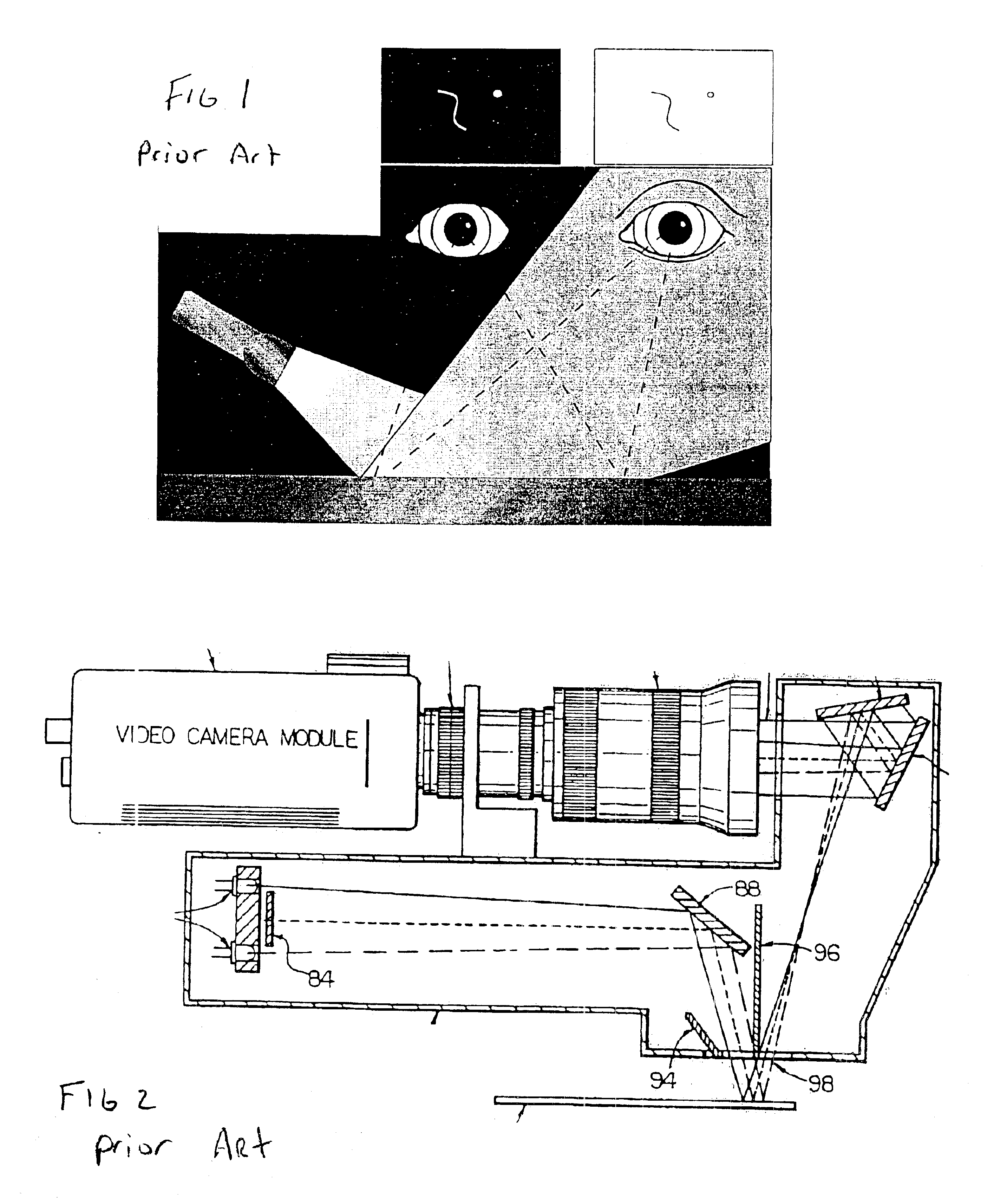
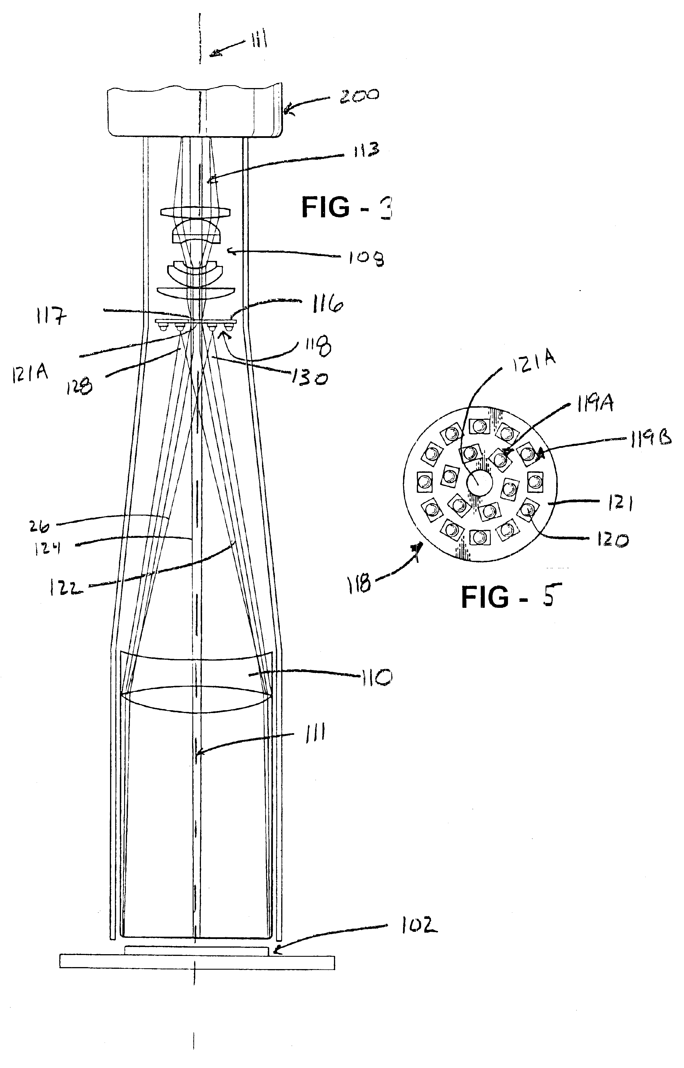
The present invention addresses the requirement to illuminate and form an image of a predominantly planar and specular surface such that the deviations from planarity or specularity of the object being imaged are reproduced with enhanced contrast. The embodiments of the present invention, as described below, utilize a telecentric lens to illuminate objects with symmetric coaxial narrow angle dark field illumination. This illumination technique is particularly suited to highlighting minor features or defects on planar specular objects. Specific examples of such objects include silicon wafers while the defects may include soft mark symbols on silicon wafers and / or edge irregularities on chip scale devices.

In particular a light source provides annular cones of light rays toward a telecentric lens. The telecentric lens redirects the light rays toward a substantially planar specular object such that the light rays are parallel and normal to the object. A property of the planar specular o...


PUM


Abstract

A coaxial narrow angle dark field imaging system is provided. The system utilizes a telecentric lens to illuminate objects with symmetric coaxial narrow angle dark field illumination. The illumination technique is particularly suited to highlight minor features or defects on planar specular objects. In particular, the coaxial light source directs light rays towards a telecentric lens which redirects the light rays towards the substantially planar specular object. The light rays are reflected back through the telecentric lens towards a camera. To the extent that the light rays are reflected from a planar specular portion of the object the light rays are blocked by a telecentric stop. Light rays reflected from a defect or feature in the planar specular object will pass through an aperture in the stop to a camera.

Description

FIELD OF THE INVENTIONThe present invention relates to imaging optics and associated illumination systems and in particular to an apparatus which provides coaxial narrow angle dark field illumination of a planar specular object having at least one defect.BACKGROUND OF THE INVENTIONThere is a class of semiconductor products that are predominantly planar and specular (flat and shiny) and it is frequently necessary to image these devices in such way that even minor deviations from planar and specular are imaged with adequate contrast. One such class of products are semiconductor wafers which may be provided with indicia that indicate, among other things, wafer number and manufacturer. These indicia are defects in the surface of the wafer and are typically a matrix of laser etched pits. These indicia are known in the art as “soft marks”. It is necessary to image these marks to read the codes at various steps along the manufacturing process.After the devices have been singulated (general...

Claims


Application Information

Patent Timeline
IPC IPC(8): G01N21/88G02B21/10G02B21/06
CPCG02B21/10G01N21/8806G02B13/22G03B15/02G06F18/00G01N21/956
Inventor BALDWIN, LEO
Owner ELECTRO SCI IND INC
Why Eureka
Try Eureka