OLEDs doped with phosphorescent compounds

a technology of phosphorescent compounds and oleds, which is applied in the direction of discharge tube luminescnet screens, natural mineral layered products, transportation and packaging, etc., can solve the problems of narrow band at 713 nm, short shelf life of such devices, and inability to meet the needs of display applications, etc., to achieve the effect of great shelf life stability

Inactive Publication Date: 2005-03-29
THE TRUSTEES FOR PRINCETON UNIV +1
View PDF51 Cites 30 Cited by
  • Summary
  • Abstract
  • Description
  • Claims
  • Application Information

AI Technical Summary

Problems solved by technology

One of the problems with the TPP-doped device is that the narrow band at 713 nm, which comprises about 40% of the emission, is not within a range that is useful for display applications.
A second problem is that TPP-doped OLEDs are very unstable, such that the shelf life of such devices is typically very short.
Formation of such triplet states can result in a substantial loss of the excitation energy in the OLED via radiationless transitions to the ground state.
Unfortunately, though it is known that the energy from an excited triplet state may be efficiently transferred under certain circumstances to the triplet state of a molecule that phosphoresces, the phosphorescent decay rate is typically not expected to be rapid enough to be adequate for use in a display device.

Method used


Image

  • OLEDs doped with phosphorescent compounds
  • OLEDs doped with phosphorescent compounds
  • OLEDs doped with phosphorescent compounds

Examples


Embodiment Construction

The present invention will now be described in detail for specific preferred embodiments of the invention, it being understood that these embodiments are intended only as illustrative examples and the invention is not to be limited thereto.

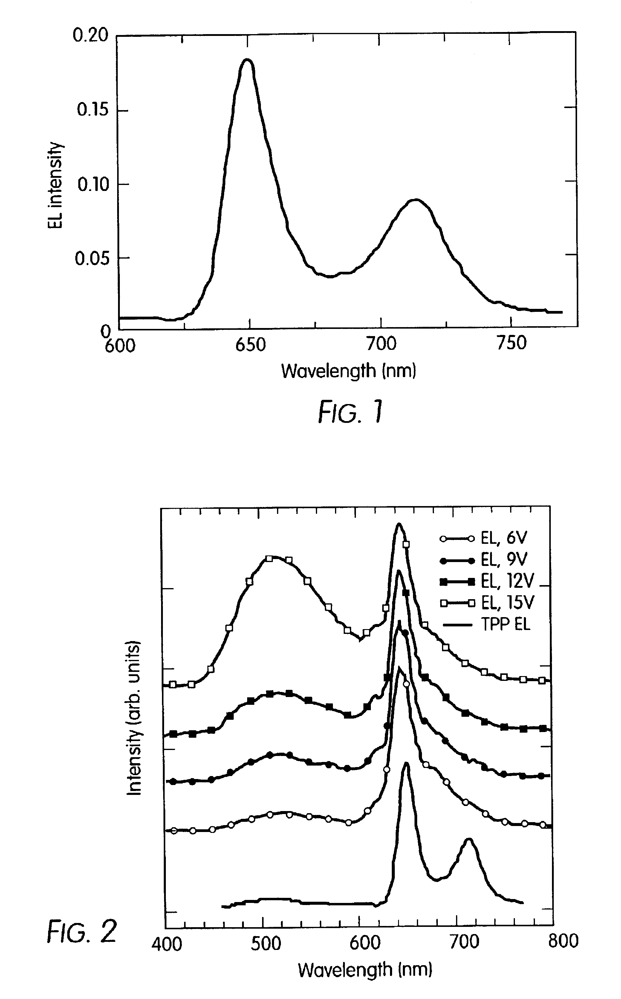
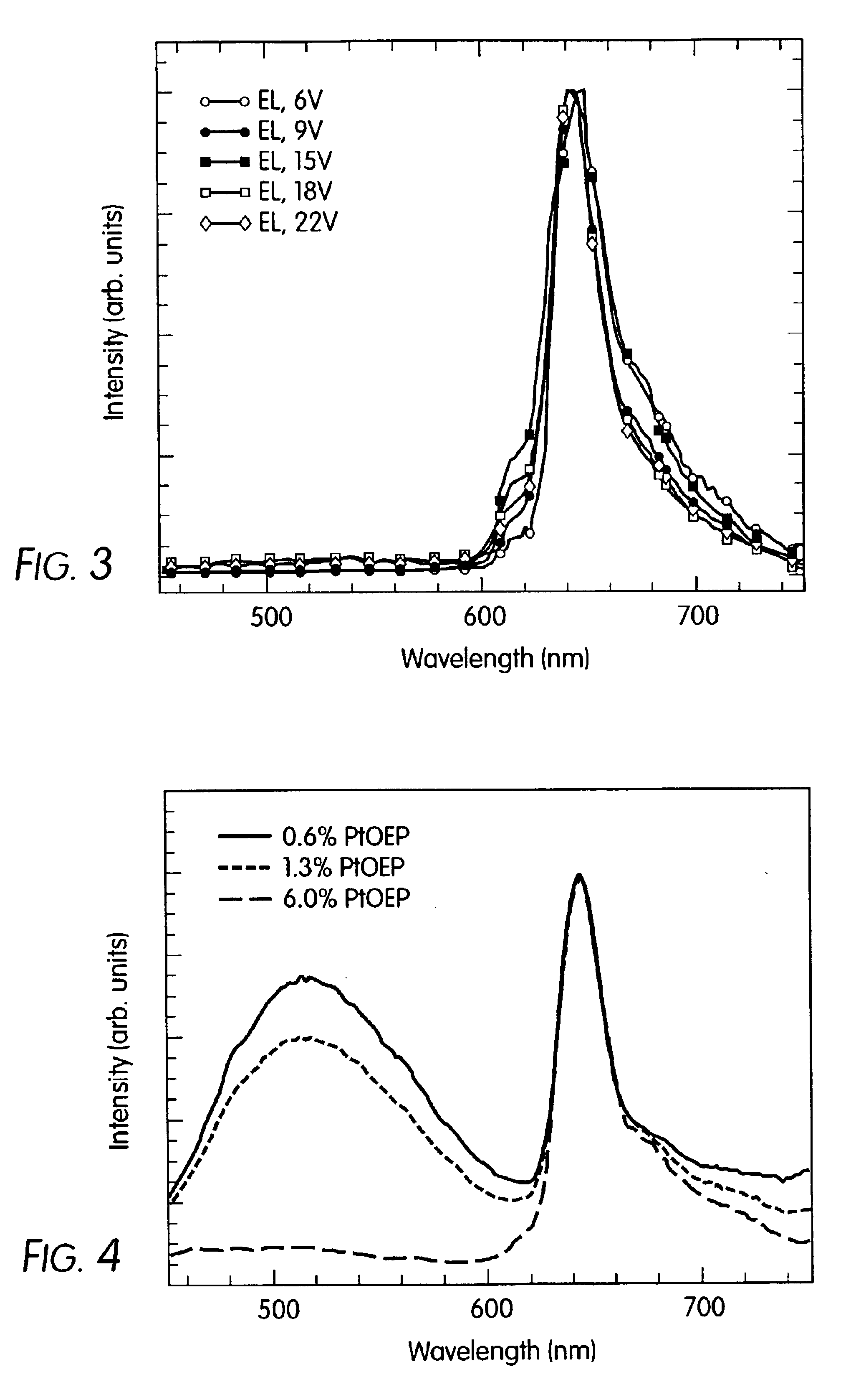
The present invention is directed to OLEDs in which emission from the device is obtained via a phosphorescent decay process wherein the phosphorescent decay rate is rapid enough to meet the requirements of a display device. As a representative embodiment of the present invention the emission layer is comprised of an emitting compound having a structure represented by Formula I:

wherein M=Pt; a=1; b=0; c=1; X=C; and R8=H; and R9=R10=Et (ethyl). In particular, this compound, platinum octaethylporphine (PtOEP), has the chemical structure of formula II:

The advantage of selecting a dopant compound such as PtOEP as the emissive material of an OLED is based, inter alia, on two particular facts. First, the photoluminescent quantum yield for this molecule ...


PUM

PropertyMeasurementUnit
transparencyaaaaaaaaaa
temperatureaaaaaaaaaa

Abstract

Organic light emitting devices are disclosed which are comprised of a heterostructure for producing electroluminescence wherein the heterostructure is comprised of an emissive layer containing a phosphorescent dopant compound. For example, the phosphorescent dopant compound may be comprised of platinum octaethylporphine (PtOEP), which is a compound having the chemical structure with the formula:

Description

FIELD OF INVENTIONThe present invention is directed to organic light emitting devices (OLEDS) comprised of emissive layers that contain a phosphorescent dopant compound.BACKGROUND OF THE INVENTIONOrganic light emitting devices (OLEDs) are comprised of several organic layers in which one of the layers is comprised of an organic material that can be made to electroluminesce by applying a voltage across the device, C. W. Tang et al., Appl. Phys. Lett 51, 913 (1987). Certain OLEDs have been shown to have sufficient brightness, range of color and operating lifetimes for use as a practical alternative technology to LCD-based full color flat-panel displays (S. R. Forrest, P. E. Burrows and M. E. Thompson, Laser Focus World, February 1995). Since many of the thin organic films used in such devices are transparent in the visible spectral region, they allow for the realization of a completely new type of display pixel in which red (R), green (G), and blue (B) emitting OLEDs are placed in a ve...

Claims


Application Information

Patent Timeline
Patent Type & Authority Patents(United States)
IPC IPC(8): C07D487/00C07D487/22C09K11/06H01L51/52H01L51/50H01L51/05H01L51/30H05B33/28H05B33/26H01L51/00
CPCC07D487/22H01L51/0067H01L51/0077H01L51/0081H01L51/0084H01L51/0087H01L51/5016H01L51/5221H05B33/14H05B33/28C09K11/06Y10T428/24942C09K2211/10C09K2211/1003C09K2211/1007C09K2211/1018C09K2211/1029C09K2211/1033C09K2211/1074C09K2211/18C09K2211/185C09K2211/186H01L51/0053H01L2251/308H01L2251/5323Y10S428/917H10K85/621H10K85/654H10K85/30H10K85/341H10K85/324H10K85/346H10K50/11H10K2101/10H10K50/828H10K2102/3031H10K2102/103H10K50/82
Inventor THOMPSON, MARK E.YOU, YUJIANSHOUSTIKOV, ANDREISIBLEY, SCOTTBURROWS, PAUL E.FORREST, STEPHEN R.
Owner THE TRUSTEES FOR PRINCETON UNIV
Why Eureka
Try Eureka