

Compound and organic photoelectronic device and image sensor
a photoelectronic device and organic technology, applied in thermoelectric devices, organic compounds, organic chemistry, etc., can solve problems such as deteriorating sensitivity, and achieve the effect of improving efficiency
- Summary
- Abstract
- Description
- Claims
- Application Information
AI Technical Summary
Benefits of technology
Problems solved by technology
Method used
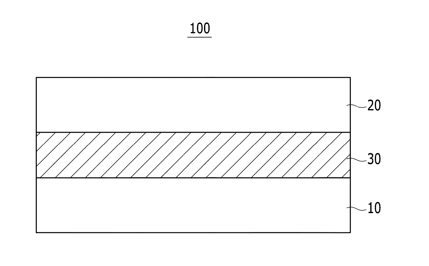
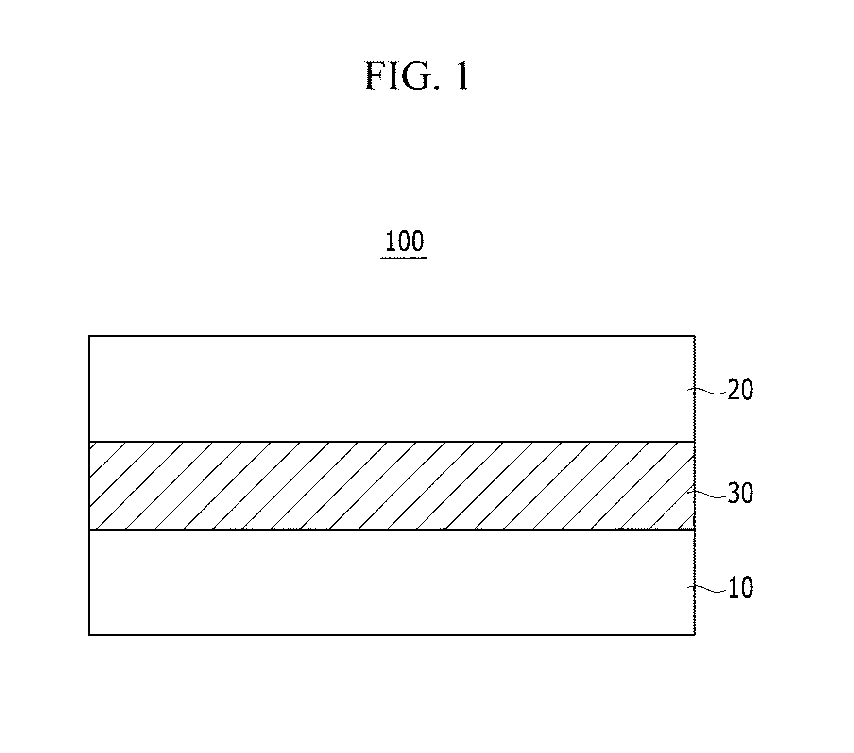
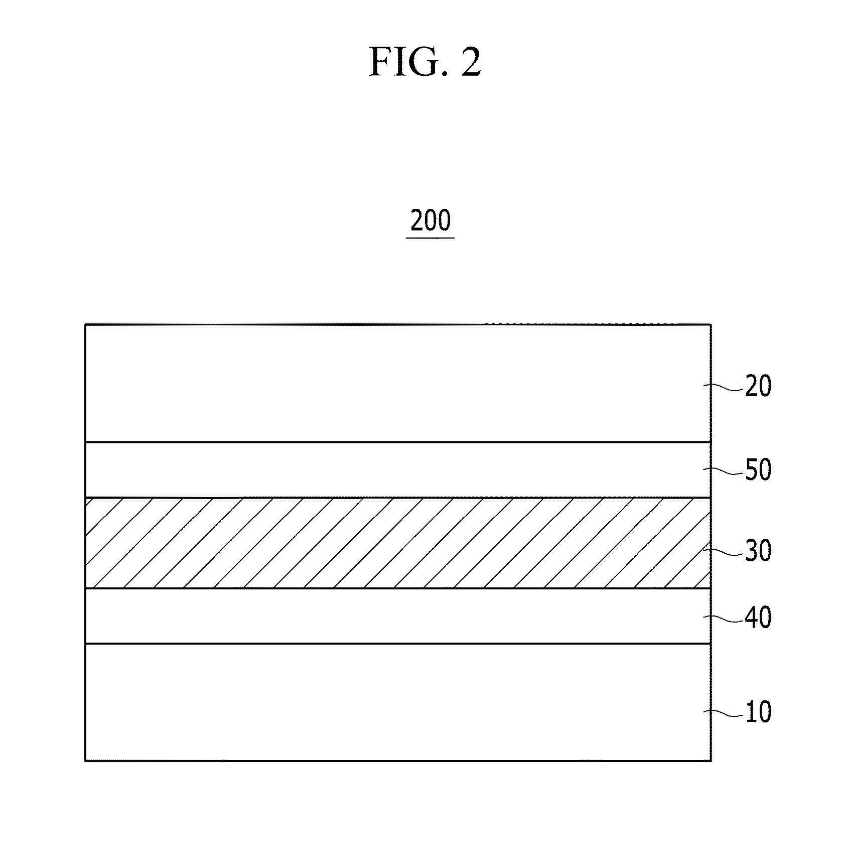
Image

Examples
synthesis example
Synthesis Example 1
[0136]
[0137]1.1 g of 2-chloro-5-benzoyl-pyrrole and 1.5 mL of POCl3 are dissolved in 60 ml of CH2Cl2, and the solution is agitated at room temperature for 3 hours. Subsequently, 2.00 g of 2,4-dimethyl-3-ethylpyrrole is added to the solution, and the mixture is additionally agitated for 36 hours and then washed and dried. The obtained material is dissolved in toluene, a small amount of triethylamine is added thereto, and the mixture is agitated at room temperature for one hour. Subsequently, 1.8 mL of BF3OEt2 is added thereto, and the mixture is reacted at 100° C. for 10 hours. Subsequently, the resultant is washed and vacuum-dried. The obtained material is dissolved in 20 ml of acetonitrile, 170 μl of propane-1-amine is added thereto, and a material obtained by refluxing the mixture for 10 hours while the mixture is agitated is recrystallized, obtaining a powder-type compound represented by the above Chemical Formula 1 m.
[0138]MALD-TOF: 409.13 (M+), 409.21 (calcul...
synthesis example 2
[0140]
[0141]A compound represented by the above Chemical Formula 1n is obtained by dissolving the compound of Example 1 in ethanol, adding malononitrile and ammonium acetate thereto, and recrystallizing a product obtained from the mixture.
[0142]MALD-TOF: 458.03 (M+), 475.22 (calculated) for C26H26BF2N5,
[0143]1H NMR (CDCl, Bruker 500 MHz): δ 1.06 (t, 3H), 1.54 (s, 3H), 1.83 (t, 3H), 2.40 (q, 2H), 2.68 (s, 3H), 4.61 (d, 2H), 6.47 (s, 1H), 7.26-7.34 (m, 2H), 7.46-7.56 (m, 3H), 8.20 (s, 1H).
synthesis example 3
[0144]
[0145]The compound of Synthesis Example 1 is dissolved in ethanol, and piperidine and ethylacetoacetate are added thereto. Subsequently, a product obtained therefrom is refluxed for 4 hours and then dried and recrystallized, obtaining a compound represented by the above Chemical Formula 10.
[0146]MALD-TOF: 475.21 (M+), 475.22 (calculated) for C27H28BF2N3O2,
[0147]1H NMR (CDCl, Bruker 500 MHz): δ 1.06 (t, 3H), 1.54 (s, 3H), 1.83 (t, 3H), 2.40 (q, 2H), 2.68 (s, 3H), 4.61 (d, 2H), 6.47 (s, 1H), 7.26-7.34 (m, 2H), 7.46-7.56 (m, 3H). 8.21 (s, 1H)
PUM
 Abstract
Description
Claims
Application Information