Leadless plastic chip carrier with etch back pad singulation and die attach pad array

Inactive Publication Date: 2005-03-29
UTAC HEADQUARTERS PTE LTD
View PDF19 Cites 76 Cited by
  • Summary
  • Abstract
  • Description
  • Claims
  • Application Information

AI Technical Summary

Benefits of technology

It is an advantage of an aspect of the present invention to mitigate internal stress between the die and the die attach pad resulting from differences in the coefficient of thermal expansion.
It is a further advantage of an aspect of the present invention to simplify printed circuit board assembly mounting. Providing an array of die attach pads rather than a

Problems solved by technology

The inner leads terminate in outer leads that are bent down to contact a mother board, thereby limiting the packaging density of such prior art devices.
During mounting of the integrated circuit package to a printed circuit board, solder alloy an the exposed contact pads and die at

Method used


Image

  • Leadless plastic chip carrier with etch back pad singulation and die attach pad array
  • Leadless plastic chip carrier with etch back pad singulation and die attach pad array
  • Leadless plastic chip carrier with etch back pad singulation and die attach pad array

Examples


Example

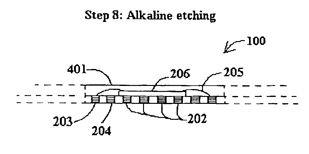
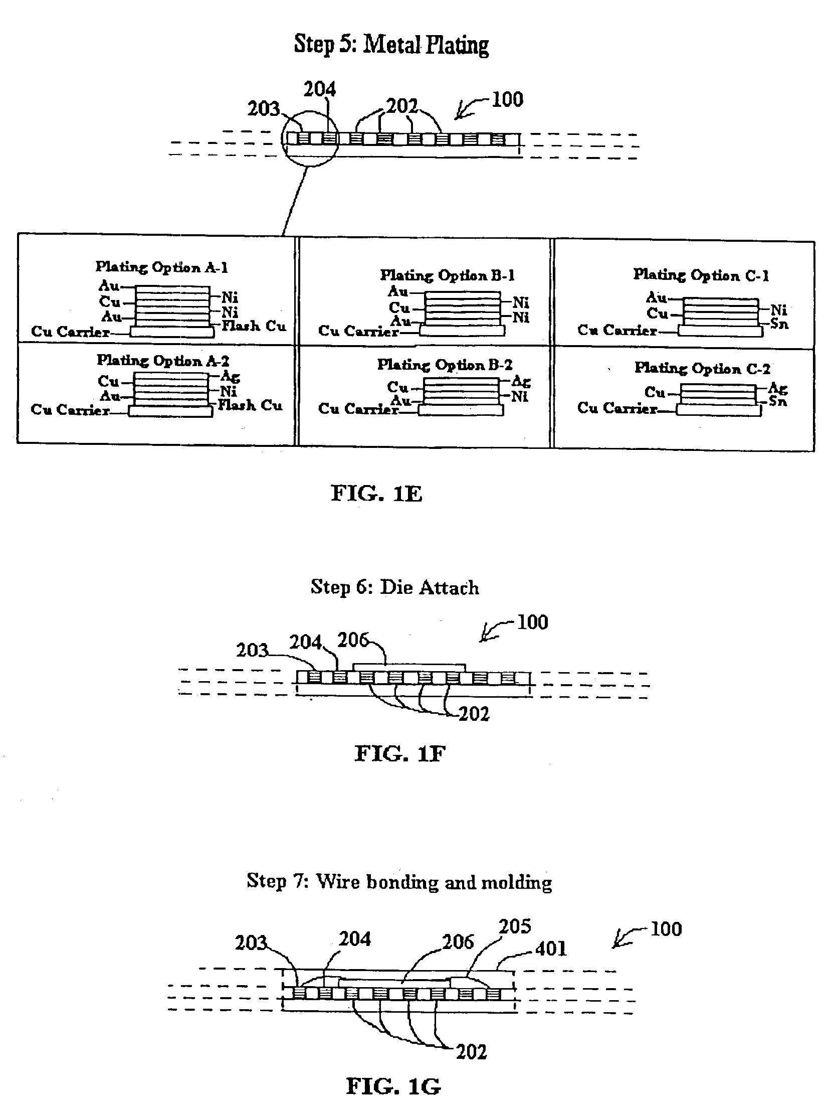
The present invention relates to an improvement over Applicant's co-pending application for a Leadless Plastic Chip Carrier With Etch Back Pad Singulation (LPCCEBS), filed concurrently herewith. Where possible, the same reference numerals have been used in this application to denote identical features described in Applicant's above-noted LPCCEBS application.

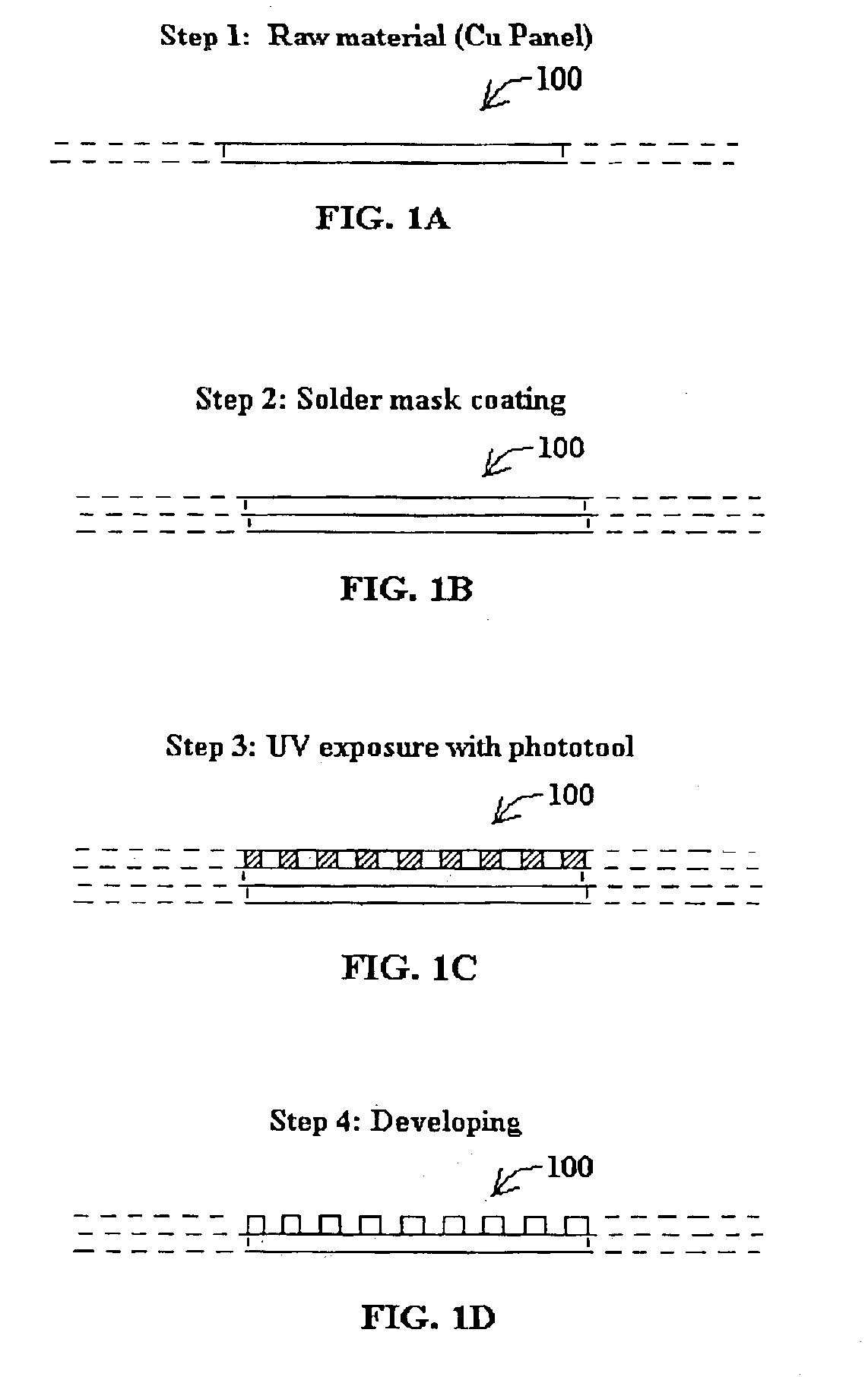
Referring to FIG. 1A, an elevation view is provided of a Cu (copper) panel substrate which forms the raw material of the leadframe strip indicated generally by the numeral 100. As discussed in greater detail in Applicants' co-pending application Ser. No. 09 / 095,803, the leadframe strip 100 is divided into a plurality of sections, each of which incorporates a plurality of leadframe units in an array (e.g. 3×3 array, 5×5 array, etc.). Only one such unit is depicted in the elevation view of FIG. 1A, portions of adjacent units being shown by stippled lines.

Referring to FIG. 1B, an upper surface of the leadframe strip 100 is coated wi...


PUM


Abstract

A leadless plastic chip carrier has a plurality of die attach pads on which a singulated semi-conductor die is mounted. At least one row of contact pads circumscribes the plurality of die attach pads and a power/ground ring is intermediate the contact pads and the die attach pads. Wire bonds connect the semiconductor die, the contact pads and the power/ground ring. An overmold covers the semi-conductor die, the die attach pads, the power/ground ring and the contact pads such that each of the die attach pads and the contact pads has one exposed surface.

Description

FIELD OF THE INVENTIONThe present invention relates in general to integrated circuit packaging, and more particularly to an improved process for fabricating a leadless plastic chip carrier which includes a post mold each back step and a unique die attach pad design.BACKGROUND OF THE INVENTIONAccording to well known prior art IC (integrated circuit) packaging methodologies, semiconductor dice are singulated and mounted using epoxy or other conventional means onto respective die pads (attach paddles) of a leadframe strip. Traditional QFP (Quad Flat Pack) packages incorporate inner leads which function as lands for wire bonding the semiconductor die bond pads. These inner leads typically require mold locking features to ensure proper positioning of the leadframe strip during subsequent molding to encapsulate the package. The inner leads terminate in outer leads that are bent down to contact a mother board, thereby limiting the packaging density of such prior art devices.In order to ove...

Claims


Application Information

Patent Timeline
IPC IPC(8): H01L23/495H01L23/31H01L23/28H01L21/02H01L23/48H01L21/48
CPCH01L21/4832H01L23/3107H01L23/49541H01L23/49548H01L24/97H01L2224/45144H01L2924/01033H01L2924/01006H01L2224/48091H01L2924/01027H01L2924/01029H01L2924/01047H01L2924/01078H01L2924/01079H01L2924/01082H01L2924/14H01L24/48H01L2924/01005H01L2924/00014H01L2924/00H01L24/45H01L2924/15747H01L2924/181
Inventor KWAN, KIN PUILAU, WING HIMTSANG, KWOK CHEUNGFAN, CHUN HOMCLELLAN, NEIL
Owner UTAC HEADQUARTERS PTE LTD
Why Eureka
Try Eureka