

Scanning electron microscope
a scanning electron microscope and electron microscope technology, applied in the field of scanning electron microscope, can solve the problems of reducing the resolution power of the sem, difficult observation at a high magnification, and extraordinary contrast of images, so as to reduce the charging up of specimens, reduce the chromatic aberration, and achieve high resolution. the effect of high resolution
- Summary
- Abstract
- Description
- Claims
- Application Information
AI Technical Summary
Benefits of technology
Problems solved by technology
Method used
Image

Examples
embodiment 1
[Embodiment 1]
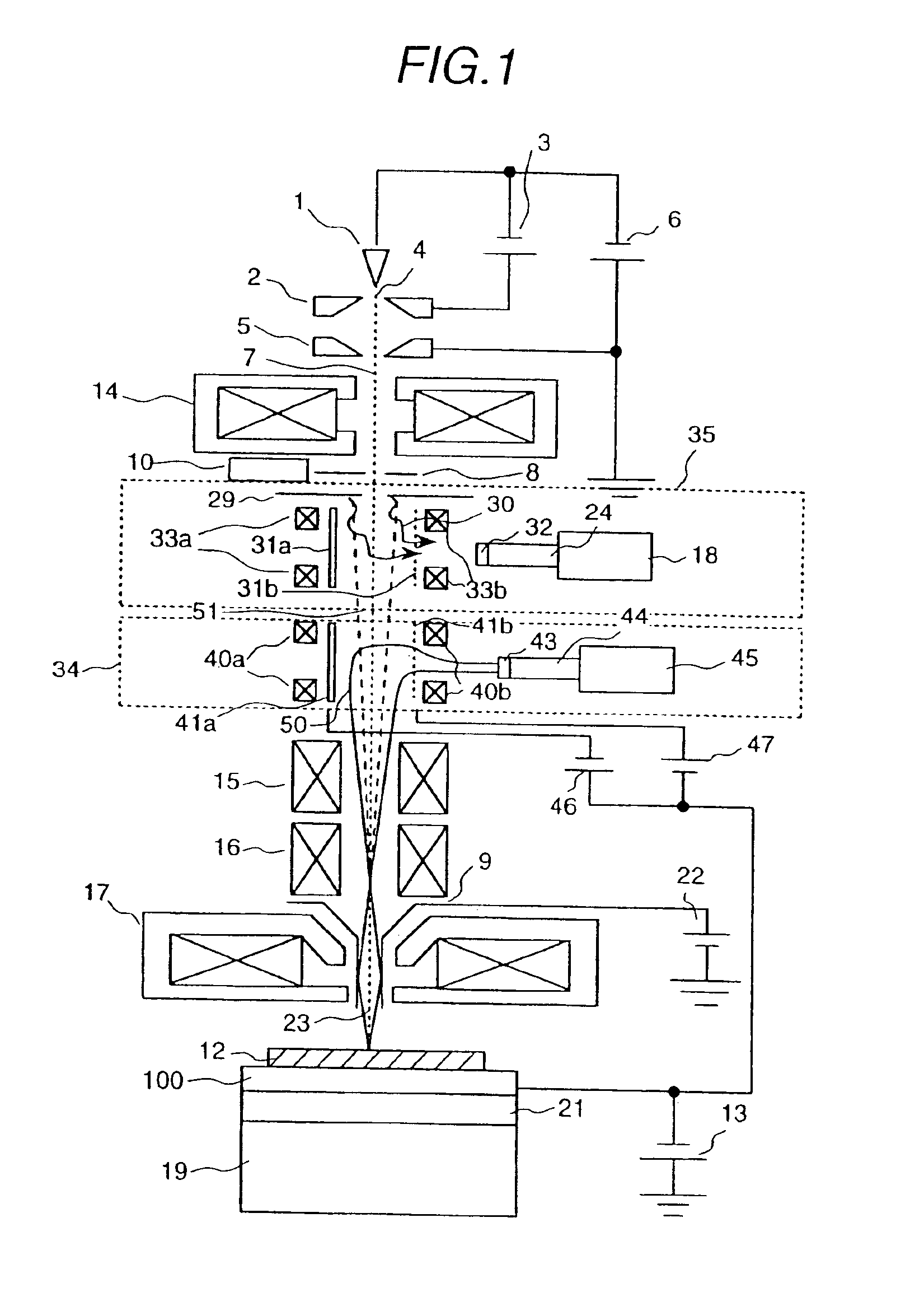
FIG. 1 is a schematic block diagram of a scanning electron microscope which is an embodiment of the present invention. When an extraction voltage 3 is applied between an electron source (electron emitting cathode 1) and the extraction electrode 2, electrons 4 are emitted from the cathode 1. The electrons 4 are accelerated (or decelerated in some cases) between the extraction electrode 2 and the anode 5 at the grounding voltage. When passing through the apertures of anode 5, the electron beam (primary electron beam 7) undergoes acceleration by the electron gun acceleration voltage 6.
The primary electron beam 7 accelerated by the anode undergoes scanning deflection by the condenser lens 14, the upper scanning deflector 15 and the lower scanning deflector 16. The upper and lower deflectors work to deflect the electron beam around the center axis of the object lens 17 to scan the object 12 to be examined (a specimen) in a 2-dimensional manner. The deflected primary electro...
embodiment 2
[Embodiment 2]
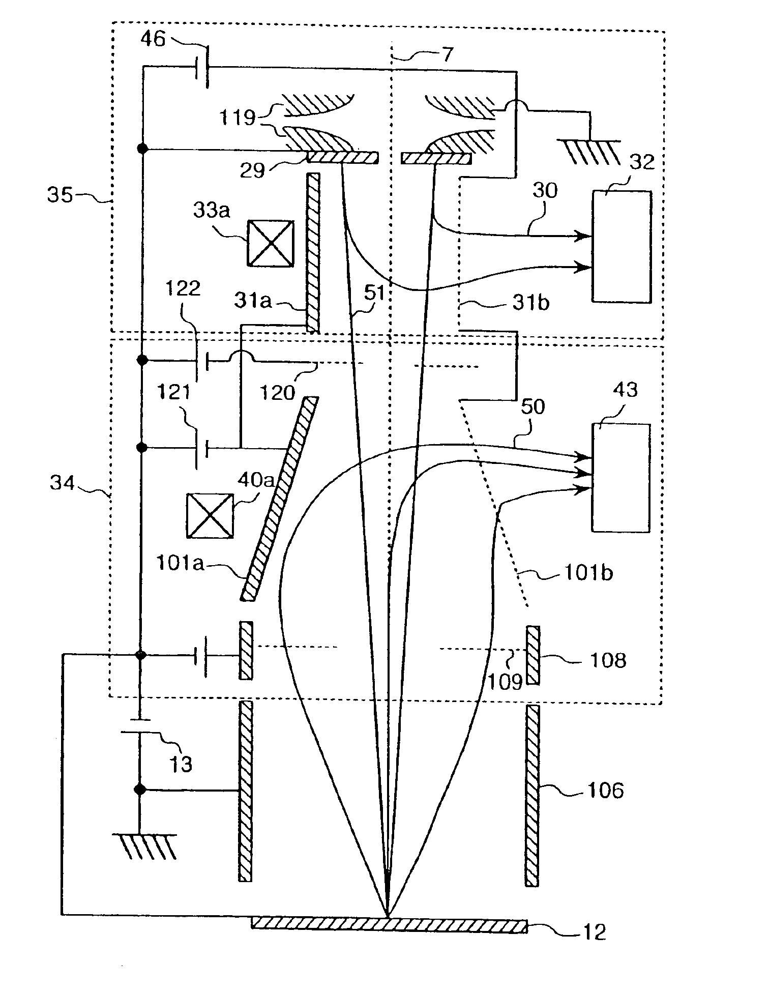
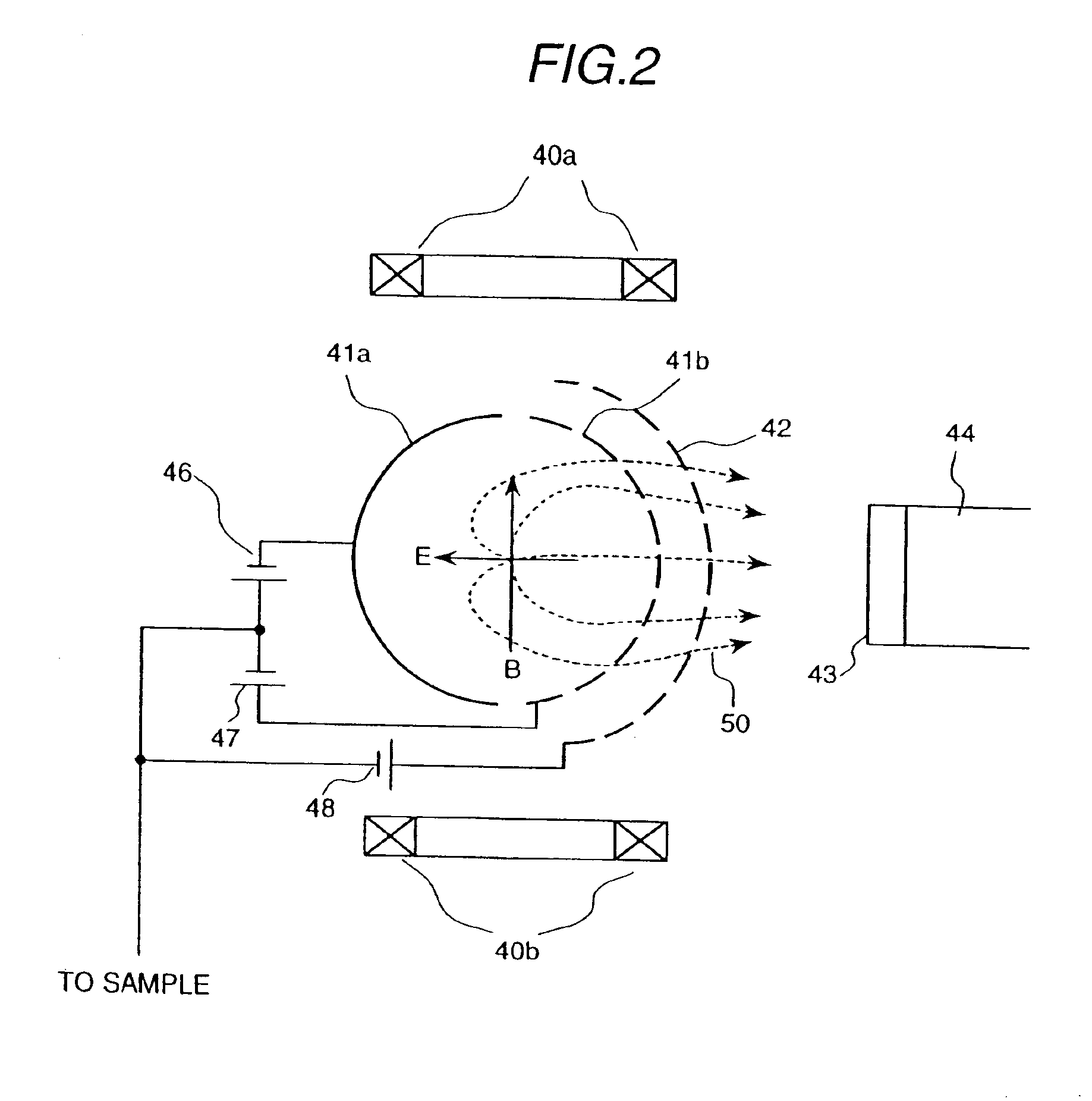
FIG. 2 shows the horizontal sectional view of the first detector which is perpendicular to the motion of a primary electron beam. The right half 41b of the cylindrical static deflector 41a and 41b is slitted longitudinally so that the deflected electrons 50 can pass through the right half 41b of the static deflector. The electric field E for deflecting secondary electrons 50 is generated by a negative deflecting voltage 46 and a positive deflecting voltage 47. Usually, these positive and negative deflecting voltages 46 and 47 are of the same magnitude. A retarding voltage is applied to their mid-point.
The deflection coils 40a and 40b produce a deflecting magnetic field B which perpendicularly intersect the electric field E. The magnitude and direction of this magnetic field can be controlled to cancel the deflection of the primary electron beam by the deflection field E.
Contrarily, this magnetic field works to deflect secondary electrons 50 further. A filtering wire gr...
embodiment 3
[Embodiment 3]
The embodiment of FIG. 1 applies a retarding voltage to the mid-point of the static deflectors 41a and 41b of the first detector 34. It is also possible to selectively detect secondary electrons of a specific energy by adding a voltage to the retarding voltage. Referring to FIG. 3, the principle of the detection will be explained below.
The configuration in FIG. 3 can selectively detect secondary electrons of a lower energy. This configuration has an upper wire grid 54 above the cylindrical static deflector 41a and 41b and a lower wire grid 55 below the static deflectors 41a and 41b. These wire grids 54 and 55 are connected to the mid-point of the deflection voltages 46 and 47 of the static deflectors 41a and 41b. This example applies a positive voltage such as 5 V to a superposition voltage 53.
In this status, the sum of the retarding voltage (negative) and the superposition voltage 53 (positive) is applied to the mid-point of the static deflectors 41a and 41b. This mak...
PUM
 Abstract
Description
Claims
Application Information