
Semiconductor films on flexible iridium substrates

a technology of iridium substrate and semiconductor film, which is applied in the direction of chemically reactive gases, chemical instruments and processes, crystal growth processes, etc., can solve the problems of inflexible srtio3 and process limitation to substrates, and process cannot be used to make continuous long lengths or wide area devices

Inactive Publication Date: 2005-03-29
UT BATTELLE LLC
View PDF40 Cites 39 Cited by
  • Summary
  • Abstract
  • Description
  • Claims
  • Application Information

AI Technical Summary

Problems solved by technology

However, such a process is limited to substrate selections available—rigid single crystal ceramic substrates such as SrTiO3.
Such a process cannot be used to make continuous long lengths or wide area devices since it is limited to the size in which SrTiO3 single crystals can be fabricated.
Moreover, SrTiO3 are not flexible.

Method used


Image

  • Semiconductor films on flexible iridium substrates
  • Semiconductor films on flexible iridium substrates
  • Semiconductor films on flexible iridium substrates

Examples


Embodiment Construction

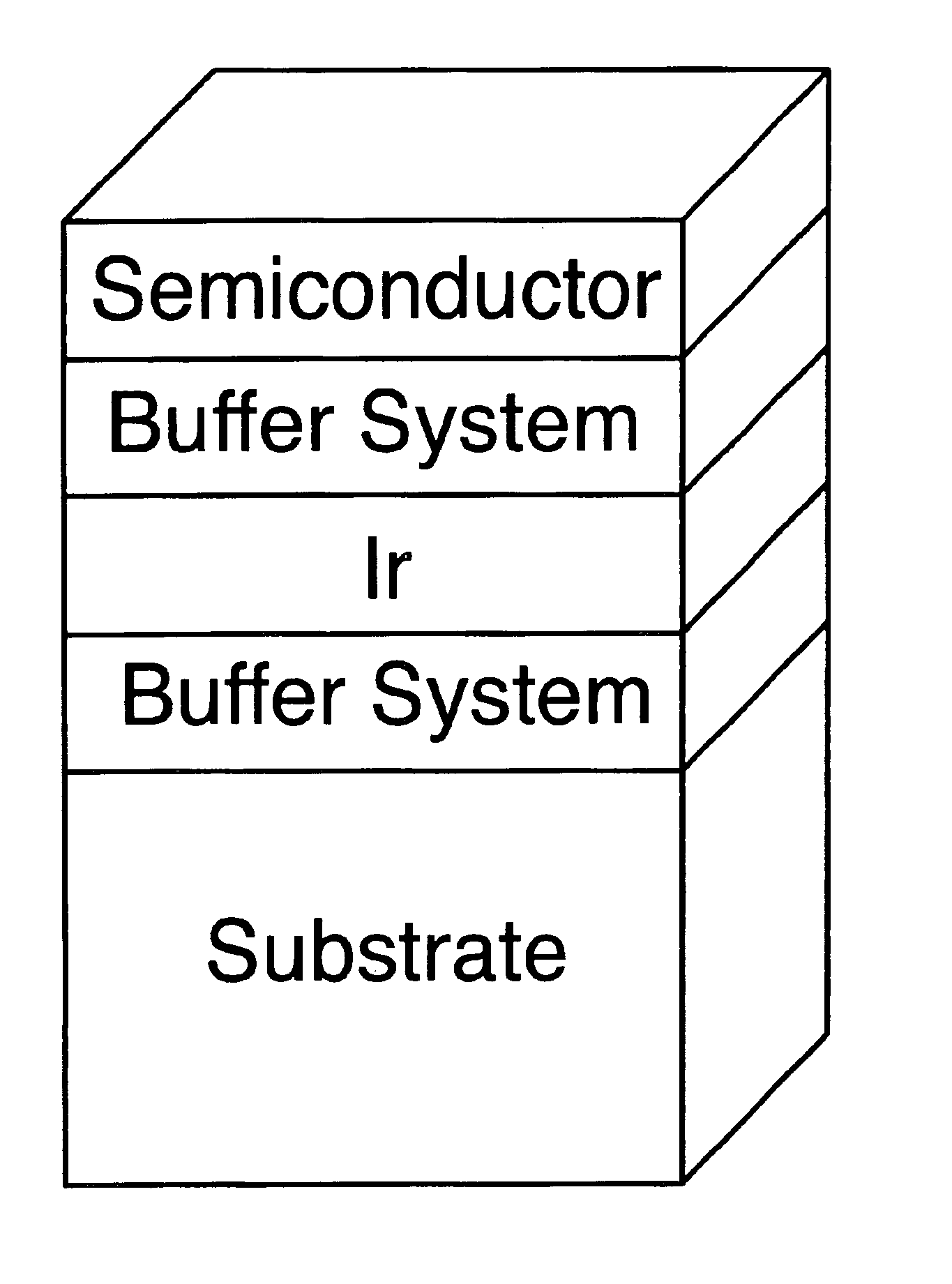
substrate; a biaxially textured Ir-based buffer layer over the flexible substrate; and at least one epitaxial layer of a semiconductor over the Ir buffer layer.

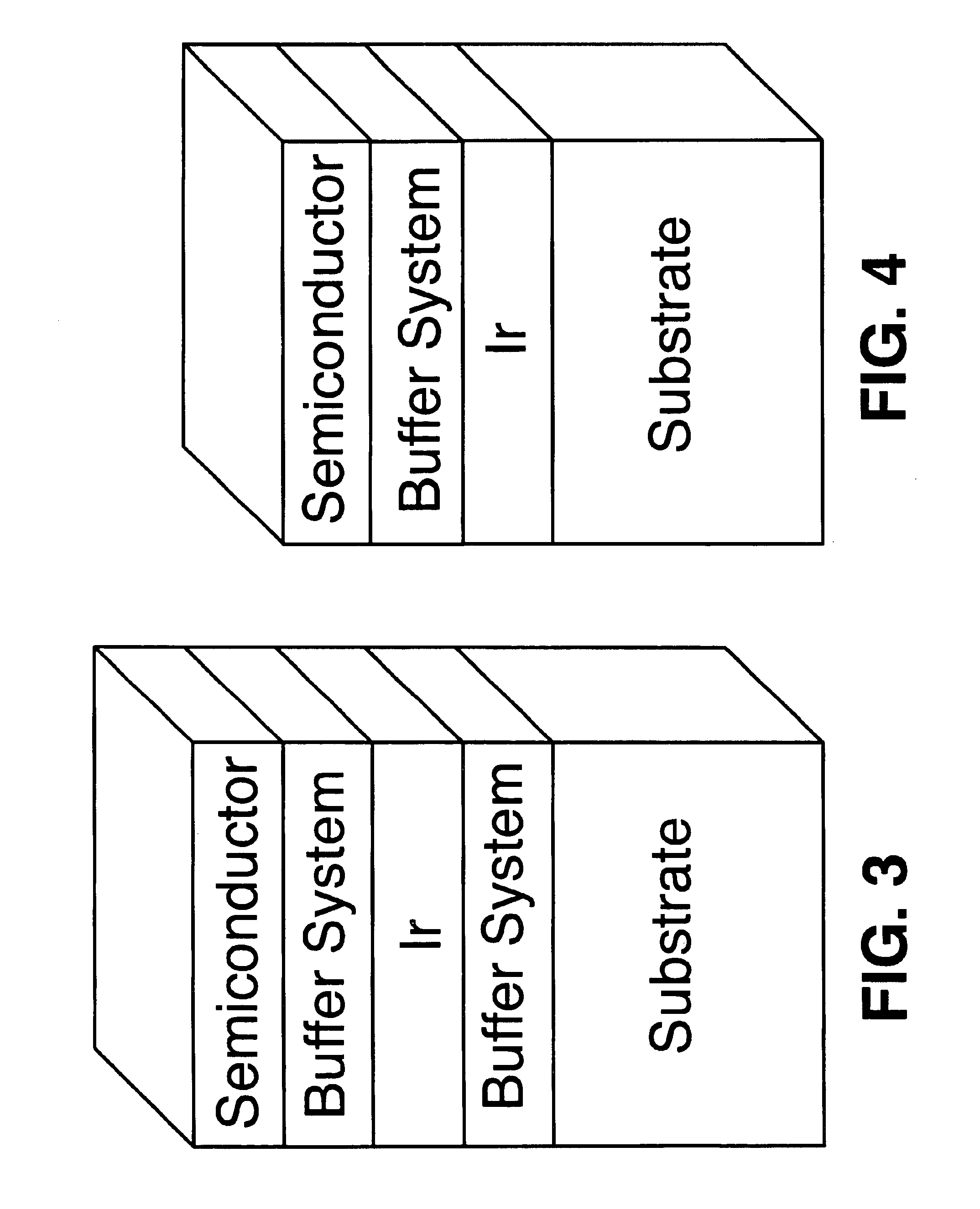
[0041]In accordance with another aspect of the present invention, a laminated semiconductor article including a flexible substrate; a biaxially textured buffer system on the flexible substrate; an epitaxial Ir-based buffer layer on the buffer system; and at least one epitaxial layer of a semiconductor over the Ir buffer layer.

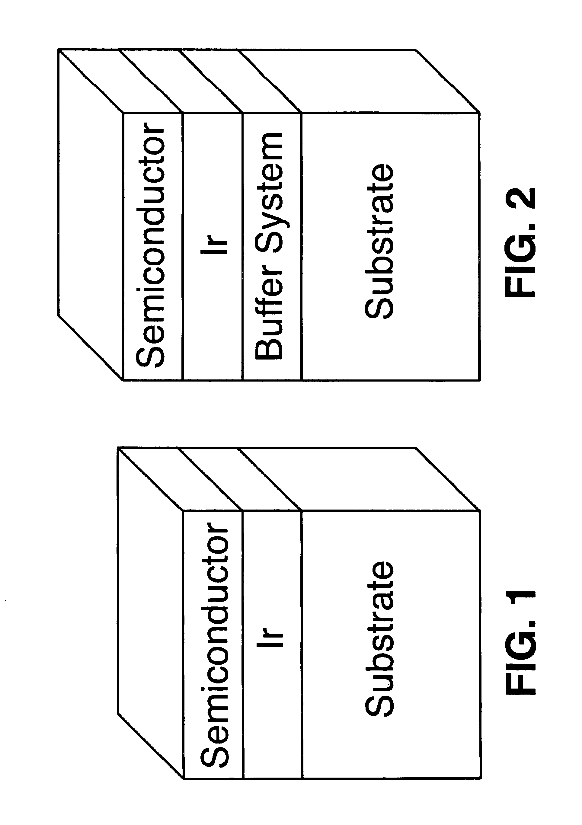
[0042]In accordance with a further aspect of the present invention, a laminated semiconductor article including a flexible Ir-based substrate; and at least one epitaxial layer of a semiconductor over the flexible Ir substrate.

BRIEF DESCRIPTION OF THE DRAWINGS

[0043]FIGS. 1-6 are schematic illustrations of various buffer layer architectures in accordance with the present invention.

[0044]For a better understanding of the present invention, together with other and further objects, advantages and capabilities...


PUM


Abstract

A laminate semiconductor article includes a flexible substrate, an optional biaxially textured oxide buffer system on the flexible substrate, a biaxially textured Ir-based buffer layer on the substrate or the buffer system, and an epitaxial layer of a semiconductor. Ir can serve as a substrate with an epitaxial layer of a semiconductor thereon.

Description

[0002]The United States Government has rights in this invention pursuant to contract no. DE-AC05-000R22725 between the United States Department of Energy and UT-Battelle, LLC.FIELD OF THE INVENTION[0003]The present invention relates to semiconductor films, and more particularly to biaxially textured semiconductor films and flexible Ir-based support substrates therefor.BACKGROUND OF THE INVENTION[0004]Various electromagnetically useful materials have been applied epitaxially to biaxially textured support materials. An important class of substrates is known as rolling assisted, biaxially textured substrates (RABiTS). Biaxial texture in a substrate refers to situation when all the grains in a polycrystalline substrate are aligned within a certain angular range with respect to one another. A polycrystalline material having biaxial texture of sufficient quality for electromagnetic applications can be generally defined as being characterized by an x-ray diffraction phi scan peak of no mor...

Claims


Application Information

Patent Timeline
IPC IPC(8): H01L21/20H01L21/02C30B25/18
CPCC30B25/18H01L21/02425H01L21/02488H01L21/02521H01L21/02502H01L21/02505H01L21/02491
Inventor GOYAL, AMIT
Owner UT BATTELLE LLC
Learn More