Isotropic dry cleaning process for noble metal integrated circuit structures

a noble metal and integrated circuit technology, applied in the direction of polycrystalline material growth, crystal growth process, chemically reactive gas, etc., can solve the problems of significant residue left on the microelectronic device structure after the etching process is completed, absence of viable dry etching techniques for submicron, and preventing widespread use of these materials

Inactive Publication Date: 2001-07-03
FELLOWS RES B V +1
View PDF4 Cites 83 Cited by
  • Summary
  • Abstract
  • Description
  • Claims
  • Application Information

AI Technical Summary

Problems solved by technology

The absence of viable dry etching techniques for submicron patterning of these electrodes is a chronic problem that has threatened to retard or even prevent widespread use of these materials.
The present dry-etching approaches utilize plasmas for reactive ion etching (RIE), are chlorine-based, and result in significant residue being left on the microelectronic device structure after the etch process has been completed.
Depending on the type of structure that is being formed by the patterning, this post-etch residue may result in short circuiting, undesired topography or other deficiencies in the operation of the circuit element in subsequent use of the product microelectronic device.
Prevention of the formation of such residues may be achieved in some instances by manipulating the reactive ion

Method used


Image

  • Isotropic dry cleaning process for noble metal integrated circuit structures
  • Isotropic dry cleaning process for noble metal integrated circuit structures
  • Isotropic dry cleaning process for noble metal integrated circuit structures

Examples


Embodiment Construction

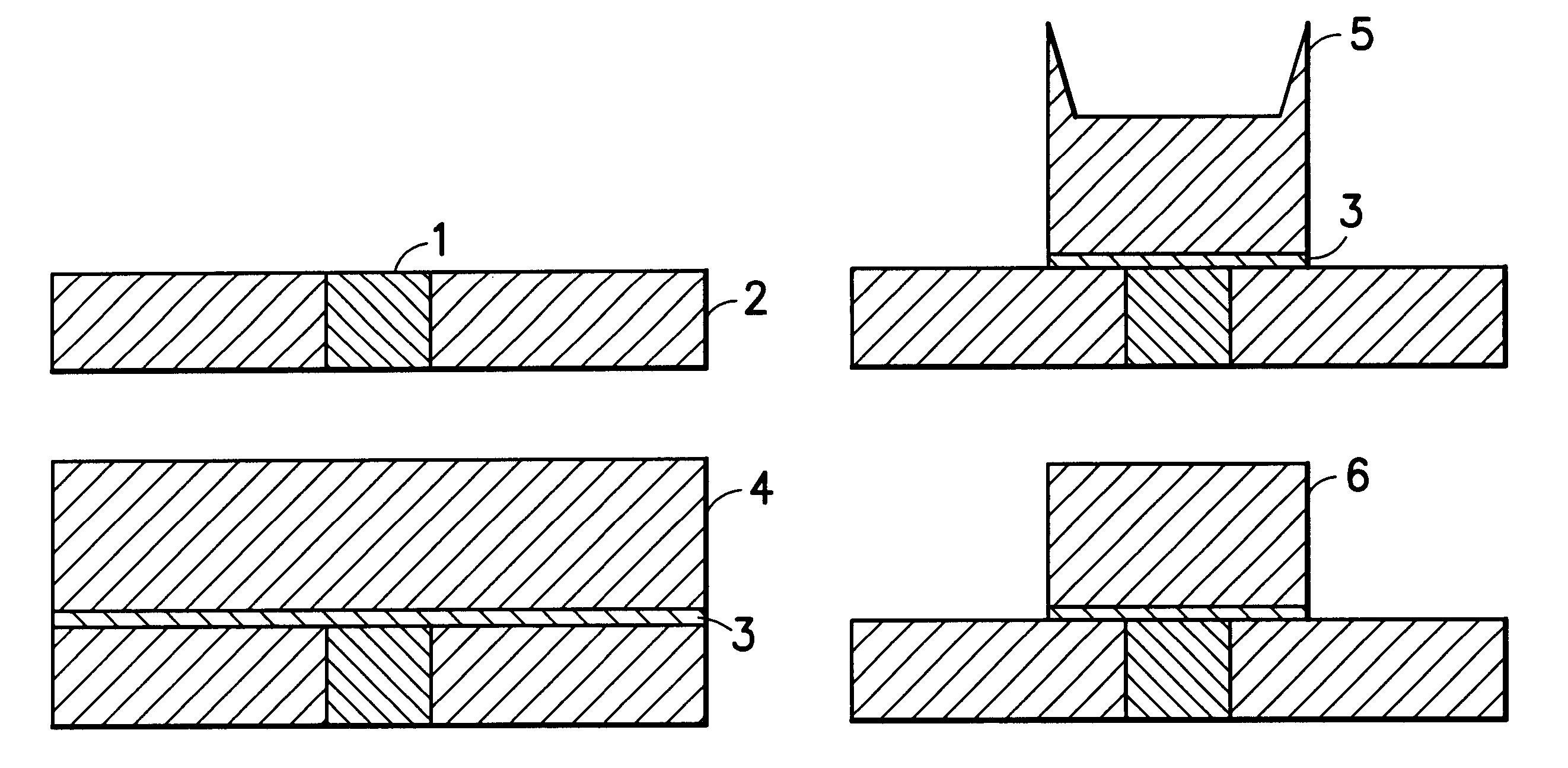
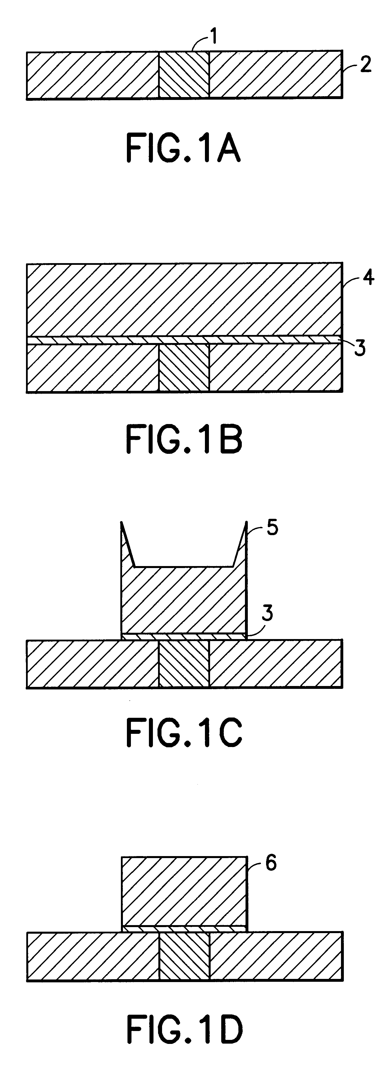
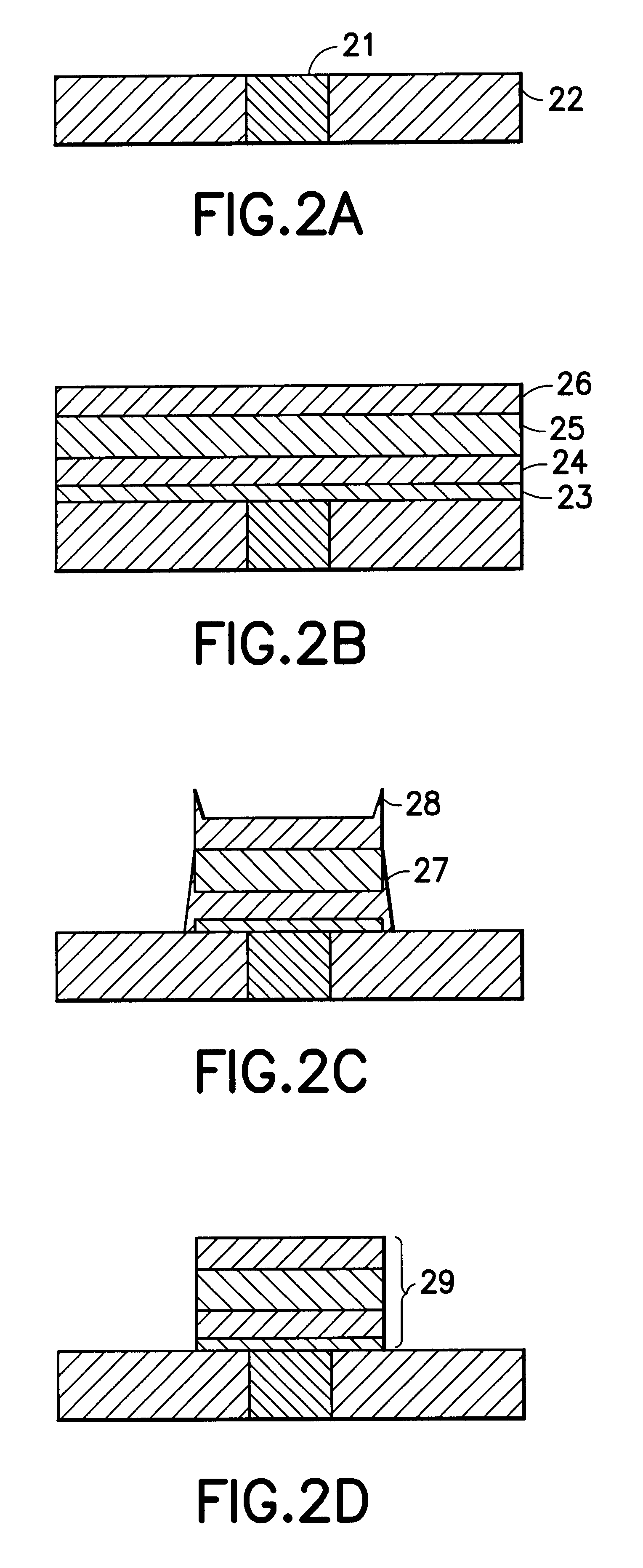
The disclosure of U.S. patent application Ser. No. 08 / 966,796 filed Nov. 10, 1997 in the names of Thomas H. Baum and Frank DiMeo, Jr. for "METHOD FOR ETCH FABRICATION OF IRIDIUM-BASED ELECTRODE STRUCTURES," is incorporated herein by reference in its entirety.

In accordance with the method of the present invention, noble metal residue is removed from a microelectronic device structure including same, by contacting the microelectronic device structure with a gas-phase reactive halide composition, e.g., XeF.sub.2, SF.sub.6, SiF.sub.4, Si.sub.2 F.sub.6, or SiF.sub.3 and / or SiF.sub.2 radicals for sufficient time and under sufficient conditions to at least partially remove the noble metal residue.

The method of the invention may be advantageously used to remove residue from a microelectronic device structure, subsequent to reactive ion etching of noble metal electrode films thereon, for patterning of the electrode in the fabrication of the microelectronic device, and / or following chemical m...


PUM

PropertyMeasurementUnit
Timeaaaaaaaaaa
Timeaaaaaaaaaa
Pressureaaaaaaaaaa

Abstract

A method for removing from a microelectronic device structure a noble metal residue including at least one metal selected from the group consisting of platinum, palladium, iridium and rhodium, by contacting the microelectronic device structure with a cleaning gas including a reactive halide composition, e.g., XeF2, SF6, SiF4, Si2F6 or SiF3 and SiF2 radicals. The method may be carried out in a batch-cleaning mode, in which fresh charges of cleaning gas are successively introduced to a chamber containing the residue-bearing microelectronic device structure. Each charge is purged from the chamber after reaction with the residue, and the charging/purging is continued until the residue has been at least partially removed to a desired extent. Alternatively, the cleaning gas may be continuously flowed through the chamber containing the microelectronic device structure, until the noble metal residue has been sufficiently removed.

Description

1. Field of the InventionThe present invention relates to an isotropic dry cleaning process for noble metal integrated circuit structures.2. Description of the Related ArtThin films of noble metals (Pt, Pd, Ir, Rh) have become technologically important in integrated circuits (ICs) as electrodes for ferroelectric and high .epsilon. thin films in FeRAMs, DRAMs, RF and microwave MMICs, pyroelectric IR focal plane detector arrays, etc.The absence of viable dry etching techniques for submicron patterning of these electrodes is a chronic problem that has threatened to retard or even prevent widespread use of these materials. The present dry-etching approaches utilize plasmas for reactive ion etching (RIE), are chlorine-based, and result in significant residue being left on the microelectronic device structure after the etch process has been completed.Depending on the type of structure that is being formed by the patterning, this post-etch residue may result in short circuiting, undesired ...

Claims


Application Information

Patent Timeline
IPC IPC(8): C07F15/00C23F1/30C23C16/18C23F1/10C23C16/40C30B25/02H01L21/02H01L21/3213H01L21/28H01L21/285
CPCC07F15/004C23C16/18C23C16/40C23F1/30C30B25/02H01L21/02071H01L28/65C30B29/16C30B29/02Y10S438/906H01L28/55H01L21/32136
Inventor VAN BUSKIRK, PETER C.DIMEO, JR., FRANKKIRLIN, PETER C.BAUM, THOMAS H.
Owner FELLOWS RES B V
Why Eureka
Try Eureka