Field emission display

a field emission display and display technology, applied in the field of display, can solve the problems of inability to achieve proportional reduction, structure is difficult to suppress a significant voltage drop with increase in screen size, and is not suitable for scanning lines

Inactive Publication Date: 2005-03-29
HITACHI LTD
View PDF4 Cites 31 Cited by
  • Summary
  • Abstract
  • Description
  • Claims
  • Application Information

AI Technical Summary

Benefits of technology

In a second invention to achieve the above object, the second electrode forming the hot electron type electron source consists of a multi layer wire structural body formed by stacked layers of a top electrode bus line upper layer including a metal film having a sheet resistance lower than that of the first electrode and a top electrode bus line lower layer electrically contacted with the top electrode.
In a third invention to achieve the above object, the second electrode forming the hot electron type electron source is made of a metal film having a sheet resistance lower than that of the first electrode and its edge is of a taper structure to be electrically contacted with the top electrode.
In a fourth invention to achieve the above object, the bottom electrode is of Al or an Al alloy such as Al—Nd, the electron accelerator of an insulator thin film is of an insulator thin film which anodic oxidizes the surface layer part of the bottom electrode, the top electrode is of a noble metal such as Ir, Pt or Au, the top electrode bus line lower layer is of a high melting point metal of Ti, Zr, Hf, V, Nb, Ta, Cr, Mo, W or an alloy thereof, and the top electrode bus line upper layer is of Al or an Al alloy having a film thickness larger than that of the top electrode bus line lower layer or Au, Ag, Ni, Cu or an alloy thereof having a resistivity lower than that of Al or an Al alloy.

Problems solved by technology

Since the sheet resistance is inevitably high as above 100 Ω / square, it is not suitable for the scan line.
It has been gradually apparent that this structure is difficult to suppress a significant voltage drop with increase in screen size.
The lower limit is limited so that proportional reduction cannot be made.
Change of it to other materials cannot be made.
The roughness of the film surface is deteriorated to impair the reliability of the tunneling insulator.
(c) When the film thickness is increased, the aluminum wire easily produces hillocks or voids in a heat treatment process.

Method used


Image

  • Field emission display
  • Field emission display
  • Field emission display

Examples


embodiment 1

<Embodiment 1>

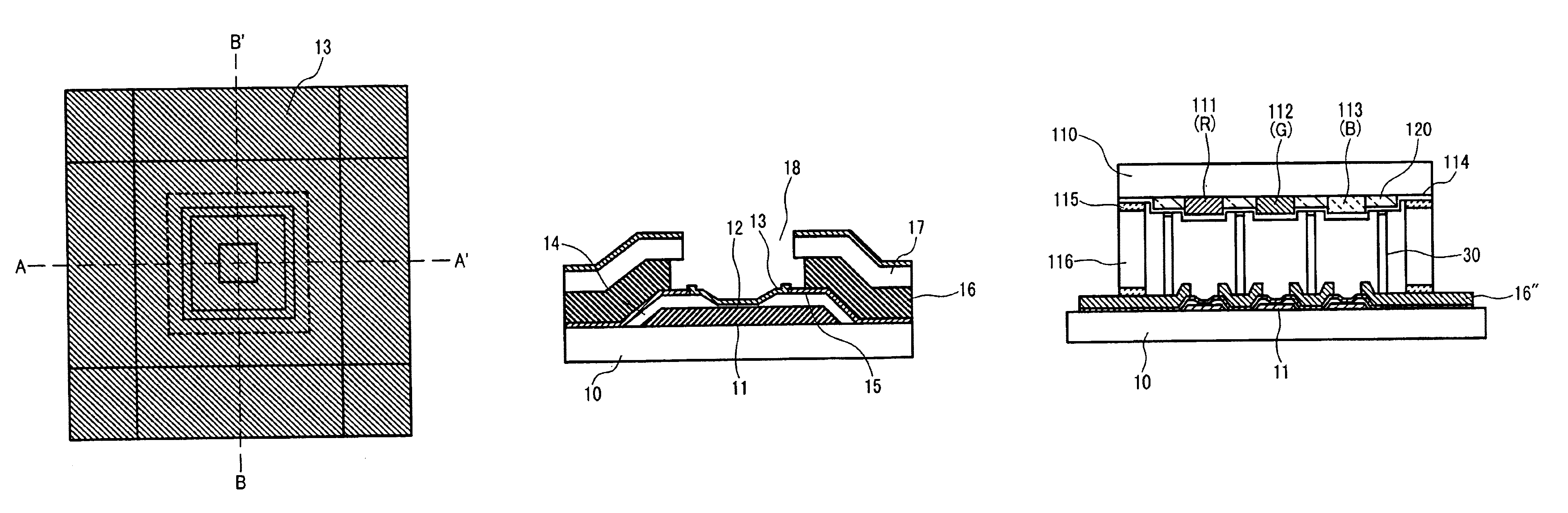
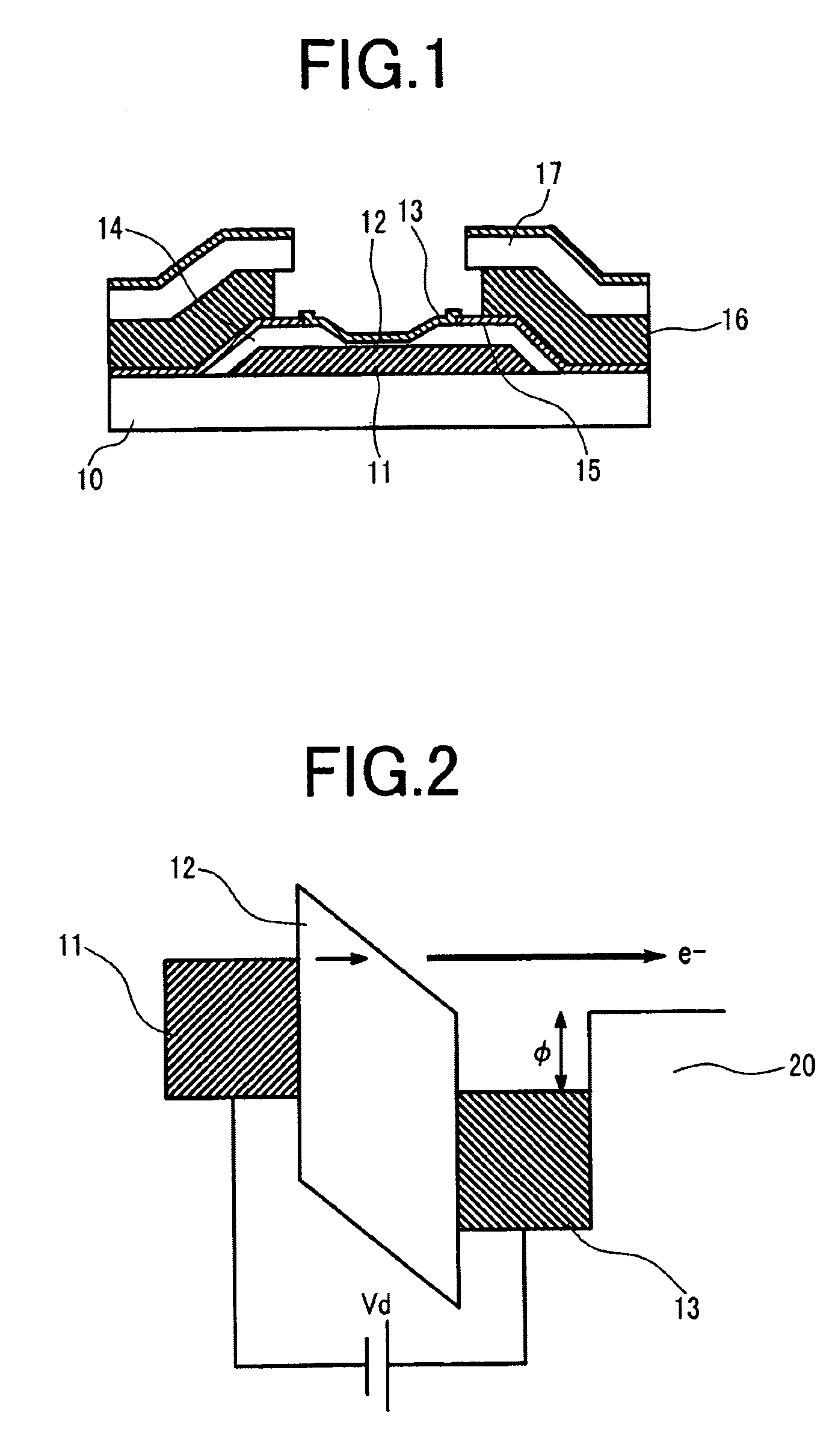
A first Embodiment of the present invention will be described using FIGS. 3 to 12 showing a method for manufacturing an MIM type electron source. As shown in FIG. 12 later describing the structure of the MIM type electron source finally obtained by the manufacturing method, there is disclosed a manufacturing method when a top electrode 13 is electrically contacted with a top electrode bus line lower layer 15 and the top electrode bus line lower layer 15 is backed by a top electrode bus line upper layer 16 of aluminum or an aluminum alloy thicker than a bottom electrode 11.

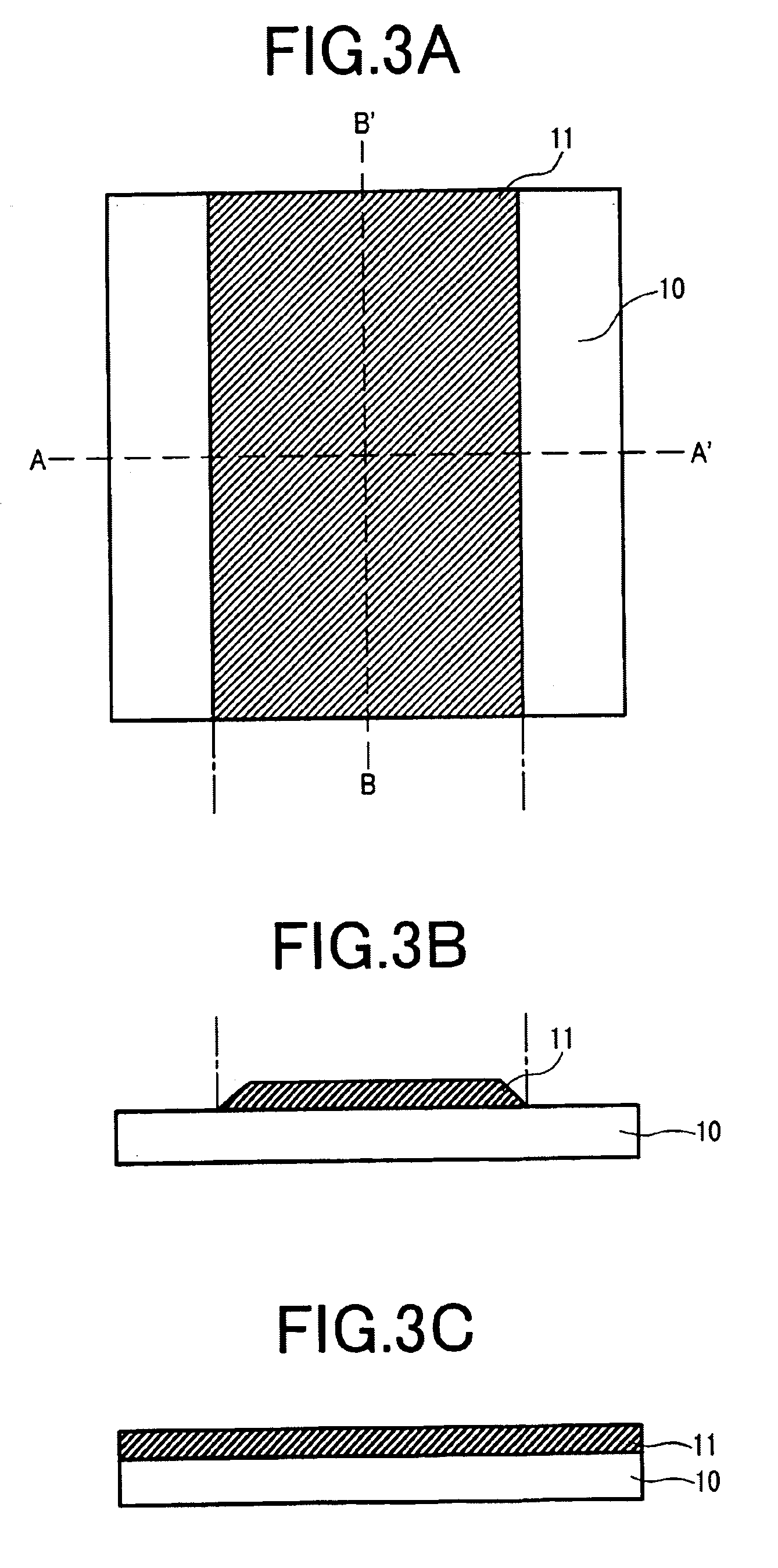
As shown in FIG. 3, a metal film for the bottom electrode 11 is deposited on an insulating substrate 10 such as glass. FIG. 3A shows a plan view. FIG. 3B shows a cross-sectional view taken along line A-A′. FIG. 3C shows a cross-sectional view taken along line B-B′. Al or an Al alloy is used as the bottom electrode material. An Al—Nd alloy in which Nd is doped by 2 atomic weight % is used. For the...

embodiment 2

<Embodiment 2>

A second Embodiment of the present invention will be described using FIGS. 13 to 19 showing a method for manufacturing an MIM type electron source. As shown in FIG. 19 later describing the structure of the MIM type electron source finally obtained by the manufacturing method, there is disclosed a manufacturing method when a top electrode 13 is electrically contacted with a top electrode bus line lower layer 15 and the top electrode bus line lower layer 15 is backed by a top electrode bus line upper layer 16 of a metal having a resistivity lower than that of a bottom electrode 11.

According to FIGS. 3 to 5 of Embodiment 1, a tunneling insulator 12 is formed. As shown in FIG. 13, the top electrode bus line lower layer 15 and the top electrode bus line upper layer 16 are deposited in that order by sputtering. FIG. 13A shows a plan view. FIG. 13B shows a cross-sectional view taken along line A-A′. FIG. 13C shows a cross-sectional view taken along line B-B′.

As the mater...

embodiment 3

<Embodiment 3>

A third Embodiment of the present invention will be described using FIGS. 20 to 27 showing a method for manufacturing an MIM type electron source. As shown in FIG. 27 later describing the structure of the MIM type electron source finally obtained by the manufacturing method, there is disclosed a manufacturing method when the structure of Embodiment 2 is extended and a top electrode bus line upper layer 16 backing a top electrode bus line lower layer 15 is formed by plating to be thick.

In FIG. 20, Cu as a base seed film 16′ when forming the top electrode bus line upper layer 16 by plating in the later process and Cr as the top electrode bus line lower layer 15 to secure the adherability of Cu and the base are successively deposited by sputtering. The film thickness of the top electrode bus line lower layer 15 is set to be about several 10 nm as that of W of Embodiment 1.

The film thickness of the base seed film 16′ when forming the top electrode bus line upper layer...


PUM


Abstract

A display having hot electron type electron sources displaying an image by a line sequential scanning scheme is provided to prevent poor brightness uniformity along scan lines. The hot electron type electron source is provided with a top electrode bus line serving as a scan line and a bottom electrode bus line serving as a data line. The top electrode bus line has a sheet resistance lower than that of the bottom electrode. The wire sheet resistance of the scam line can be reduced to several m/square. When forming a 40 inch large screen FED using the hot electron type electron sources, a voltage drop amount produced in the scan line can be suppressed below an allowable range. As a result, high quality image without poor brightness uniformity can be obtained.

Description

BACKGROUND OF THE INVENTION1. Field of the InventionThe present invention relates to a display using cold cathode electron sources. More specifically, the present invention relates to a display suitable for an emissive type flat panel display using hot electron type electron sources.2. Description of the Related ArtA display using cold cathode electron sources which are micro and can be integrated is called an FED (Field Emission Display). The cold cathode electron source is broadly divided into a field emission electron source and a hot electron type electron source. The former includes a spindt type electron source, a surface conduction type electron source and a carbon nano-tube type electron source. The latter includes an MIM (Metal-Insulator-Metal) type electron source stacked with metal-insulator-metal and an MIS (Metal-Insulator-Semiconductor) type electron source stacked with metal-insulator-semiconductor.The MIM type electron source is disclosed in Japanese Patent Applicati...

Claims


Application Information

Patent Timeline
Patent Type & Authority Patents(United States)
IPC IPC(8): G09G3/22H01J1/30G09G3/10G11C11/24H01J1/312H01J9/02
CPCB82Y10/00H01J9/022H01J9/241H01J1/312G09G3/22H01J2201/3125H01J1/30
Inventor SAGAWA, MASAKAZUSUZUKI, MUTSUMIKUSUNOKI, TOSHIAKI
Owner HITACHI LTD
Why Eureka
Try Eureka