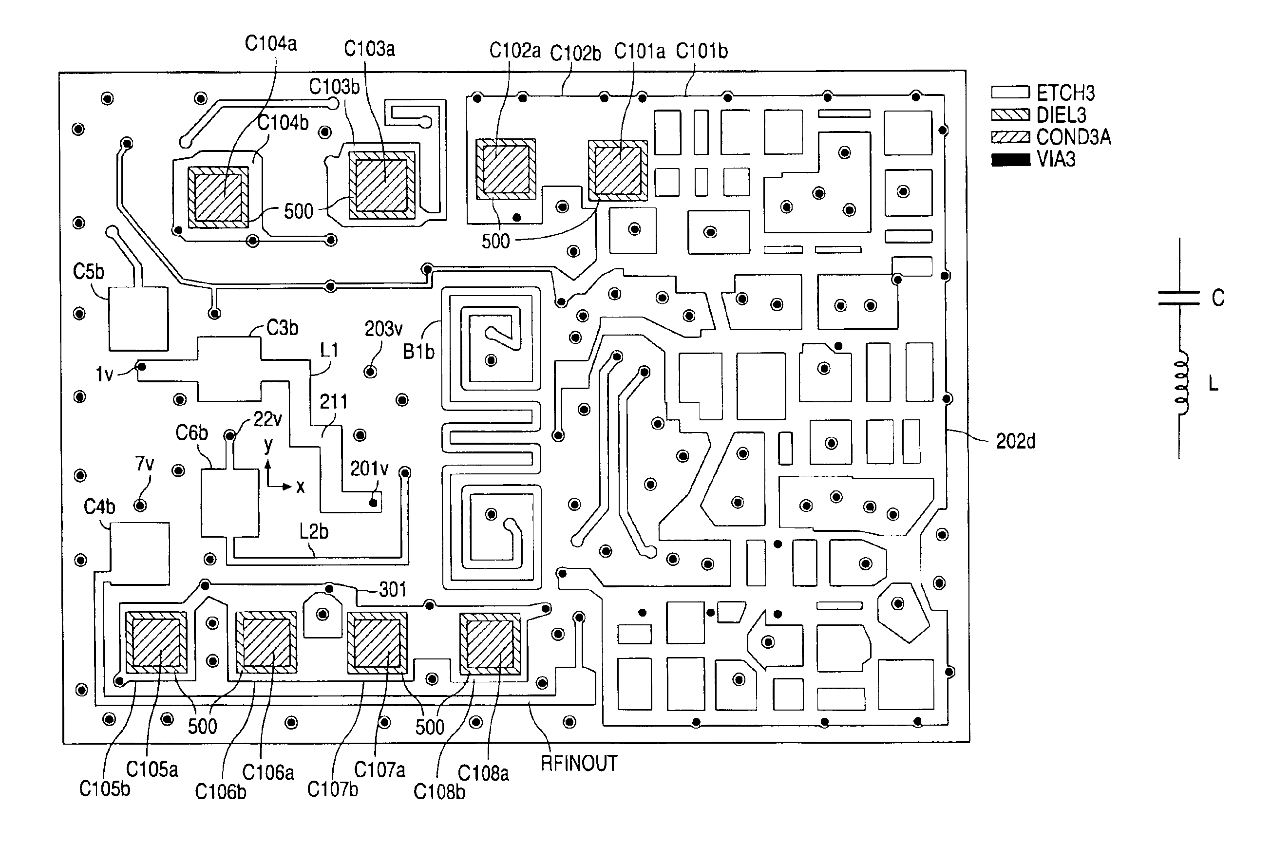
In accordance with the presently claimed invention, a multilayered, low temperature co-fired ceramic (LTCC) substrate is provided within which one or more capacitors are formed (e.g., for power supply decoupling). Self-resonance is introduced by the capacitance of each capacitor interacting with an inductance formed by the interconnects (e.g., conductive vias and other conductive interconnects among the electrode patterns) which couple such capacitor to its respective circuit electrode and interface electrode (e.g., ground reference).
In accordance with one embodiment of the presently claimed invention, self-resonant radio frequency (RF) circuitry within a multilayered low temperature co-fired ceramic (LTCC) substrate includes multiple ceramic tape layers and a plurality of conductive paths. A first ceramic tape layer includes a plurality of interface electrodes. A second ceramic tape layer includes a plurality of circuit electrodes for at least an RF integrated circuit. A plurality of intermediate ceramic tape layers positioned between the first and second ceramic tape layers include a plurality of electrode patterns. The plurality of conductive paths, each of which includes one or more conductive vias and one or more portions of selected ones of the plurality of electrode patterns, mutually couples selected ones of the pluralities of interface electrodes, circuit electrodes and electrode patterns. One of the first, second and plurality of intermediate ceramic tape layers includes: an electrode pattern with at least a portion coupled to at least one of the plurality of interface electrodes by a first one of the plurality of conductive paths; a dielectric paste deposited upon the electrode pattern portion; and a conductive plate disposed on at least a portion of the dielectric paste, thereby forming, together with the dielectric paste and electrode pattern portion, a capacitance. The conductive plate is coupled to at least one of the plurality of circuit electrodes by a second one of the plurality of conductive paths, and the first and second conductive paths together form an inductance such that the inductance and the capacitance together form a series resonant impedance at a predetermined frequency of resonance.
In accordance with another embodiment of the presently claimed invention, self-resonant radio frequency (RF) circuitry within a multilayered low temperature co-fired ceramic (LTCC) substrate includes multiple ceramic tape layers and a plurality of conductive paths. A first ceramic tape layer includes a plurality of interface electrodes. A second ceramic tape layer includes a plurality of circuit electrodes for at least an RF integrated circuit. A plurality of intermediate ceramic tape layers positioned between the first and second ceramic tape layers includes a plurality of electrode patterns. The plurality of conductive paths, each of which includes one or more conductive vias and one or more portions of selected ones of the plurality of electrode patterns, mutually couples selected ones of the pluralities of interface electrodes, circuit electrodes and electrode patterns. One of the first, second and plurality of intermediate ceramic tape layers includes: an electrode pattern with at least a portion coupled to at least one of the plurality of circuit electrodes by a first one of the plurality of conductive paths; a dielectric paste deposited upon the electrode pattern portion; and a conductive plate disposed on at least a portion of the dielectric paste, thereby forming, together with the dielectric paste and electrode pattern portion, a capacitance. The conductive plate is coupled to at least one of the plurality of interface electrodes by a second one of the plurality of conductive paths, and the first and second conductive paths together form an inductance such that the inductance and the capacitance together form a series resonant impedance at a predetermined frequency of resonance.
In accordance with still another embodiment of the presently claimed invention, self-resonant radio frequency (RF) circuitry within a multilayered low temperature co-fired ceramic (LTCC) substrate includes multiple ceramic tape layers and a plurality of conductive paths. A first ceramic tape layer includes a plurality of interface electrodes. A second ceramic tape layer includes a plurality of circuit electrodes for at least an RF integrated circuit. A plurality of intermediate ceramic tape layers positioned between the first and second ceramic tape layers includes a plurality of electrode patterns. The plurality of conductive paths, each of which includes one or more conductive vias and one or more portions of selected ones of the plurality of electrode patterns, couples among selected ones of the pluralities of interface electrodes, circuit electrodes and electrode patterns. One of the first, second and plurality of intermediate ceramic tape layers includes: an electrode pattern with at least a portion coupled by a first one of the plurality of conductive paths to one or more of the selected ones of the pluralities of interface electrodes, circuit electrodes and electrode patterns; a dielectric paste deposited upon the electrode pattern portion; and a conductive plate disposed on at least a portion of the dielectric paste, thereby forming, together with the dielectric paste and electrode pattern portion, a capacitance. The conductive plate is coupled by a second one of the plurality of conductive paths to a different one or more of the selected ones of the pluralities of interface electrodes, circuit electrodes and electrode patterns, and the first and second conductive paths together form an inductance such that the inductance and the capacitance together form a series resonant impedance at a predetermined frequency of resonance.

