
Optical devices

Inactive Publication Date: 2005-03-29
JDS UNIPHASE CORP
View PDF4 Cites 2 Cited by
  • Summary
  • Abstract
  • Description
  • Claims
  • Application Information

AI Technical Summary

Benefits of technology

[0016]Advantageously, the improvement in performance of the optical devices of the present invention follows at least in part by suppressing the rate of the non-zero DC drift behaviour of the device, which is due to imperfect electrical insulation characteristics of device constituent materials.
[0021]Preferably, embodiments are provided in which the buffer layer comprises silicon and oxygen in non-stoichiometric quantities, that is in a hyper-oxygen condition. Preferred embodiment are substantially free from intentional doping of other elements, in particular, metal elements.
[0022]To avoid inherent problems associated with the use of a complex buffer layer material, such as metal-doped SiO2, the present invention advantageously, uses simple silicon oxides as the buffer layer, which have a preferred Si / O ratio to provide a reduced DC drift.

Problems solved by technology

However, it will be appreciated that the manufacture of a buffer layer having such a complex composition is a relatively complex and expensive procedure.
The accurate control of the chemical composition of such complex oxide materials in the form of a film (i.e. the buffer layer) is very difficult because of, for example, the different volatile temperatures and pressures of the source materials, and the differences in suitable film deposition conditions being depending on materials, etc.

Method used


Image

  • Optical devices
  • Optical devices
  • Optical devices

Examples


Embodiment Construction

ng drawings in which:

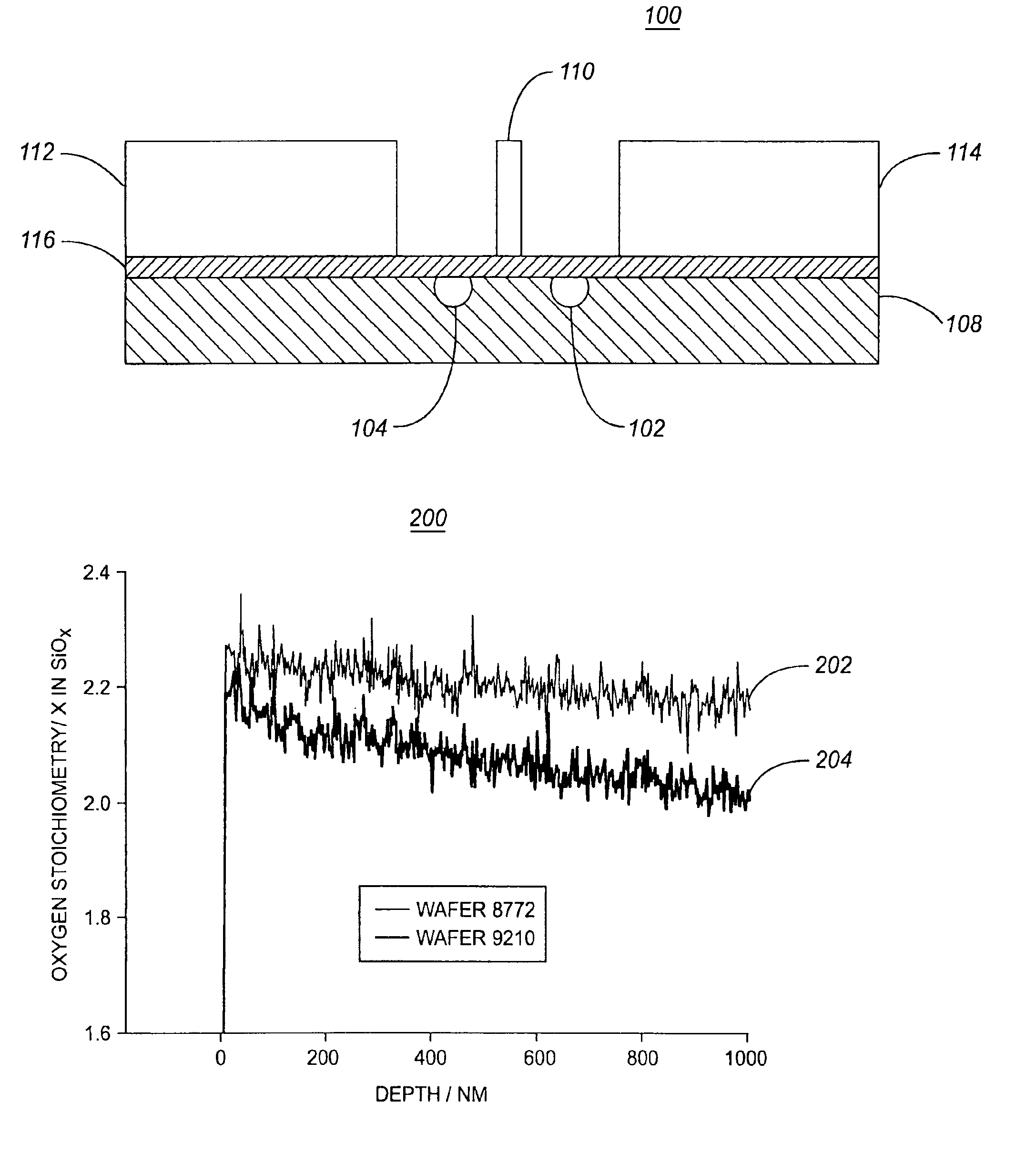
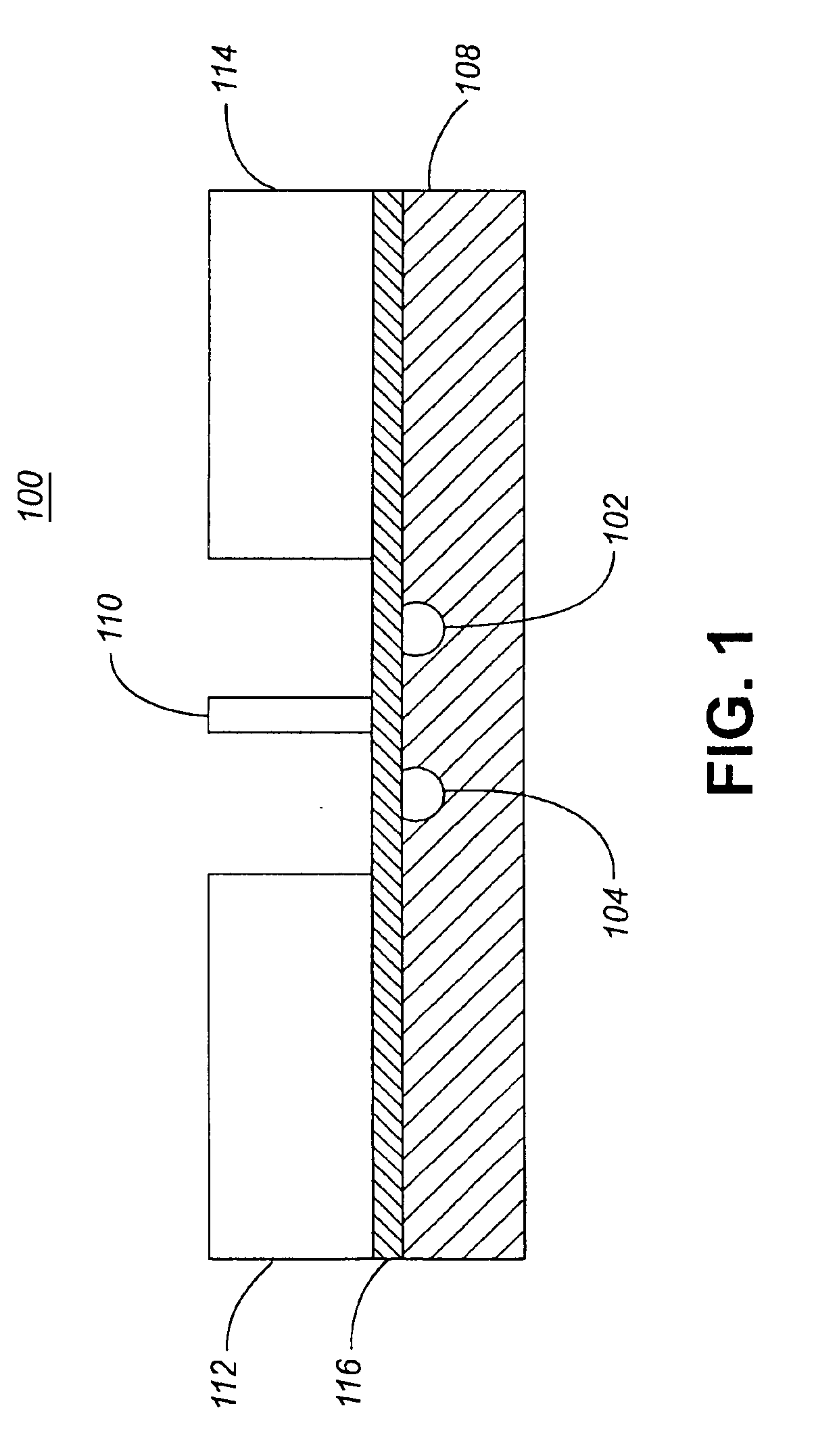
[0025]FIG. 1 depicts schematically a cross-sectional view of a Mach-Zehnder modulator;

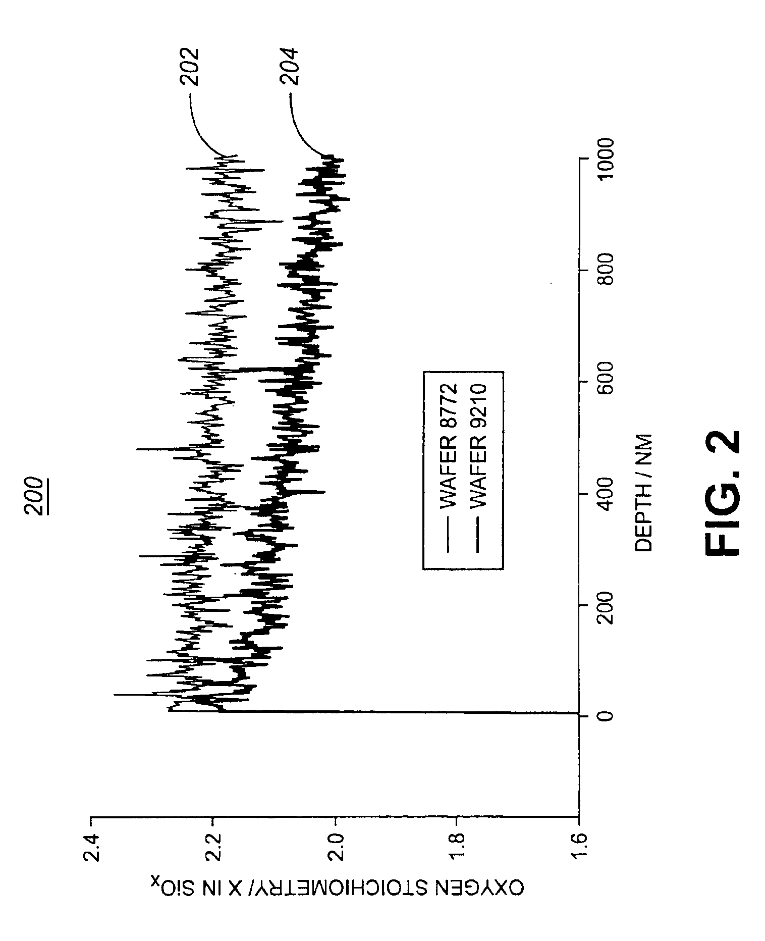
[0026]FIG. 2 shows a graph of the variation of oxygen stoichiometry with buffer layer depth for embodiments;

[0027]FIG. 3 shows a first graph of the variation of DC bias voltage with time (DC drift) for an embodiment with an SiOx buffer layer, where x is about 2.04;

[0028]FIG. 4 shows a second graph of the variation of the DC bias voltage with time (DC drift) for an embodiment with an SiOx buffer layer, where x≧2.2;

[0029]FIG. 5 depicts a log-linear relationship between the DC drift rate and the oxygen stoichiometry of the buffer layers for various embodiments of the present invention and for prior art devices; and

[0030]FIG. 6 shows a graph of the variation of impurities with buffer layer depth for an embodiment.

DESCRIPTION OF THE PREFERRED EMBODIMENTS

[0031]Referring to FIG. 1, there is shown a schematic cross-sectional view 100 of a Mach-Zehnder modulator. The waveguide arms 102 ...


PUM


Abstract

The present invention relates to optical devices and, more particularly, to optical waveguide devices in which characteristics of a light signal are modulated or changed in accordance with an applied electric field. Conventionally, in such devices, such as, for example, a Mach-Zehnder modulator, DC drift problems, as are well known within the art, must be surmounted if the optical device is to meet minimum performance criteria. Suitably the present invention provides a layer of an oxide of silicon, preferably substantially, free of metallic impurities, where the ratio of oxygen to silicon is greater than 2 and is preferably greater than or equal to 2.2.

Description

CROSS-REFERENCE TO RELATED APPLICATIONS[0002]This application claims priority of U.S. Provisional Patent Application No. 60 / 333,801 filed on Nov. 28, 2001, and United Kingdom Patent Application No: 0202738.1 filed on Feb. 6, 2002 which is incorporated herein by reference for all purposesFIELD OF THE INVENTION[0003]The present invention relates to optical devices and methods of manufacture thereof and, more particularly, to optical waveguide devices and associated methods of manufacture.BACKGROUND TO THE INVENTION[0004]Conventionally, an RF field is applied to an optical device in the region of a waveguide so as to change the refractive index of the waveguide to bring about modulation in intensity and / or phase of any light being carried within that waveguide.[0005]The modulating RF electric field is usually applied via an electrode formed on a buffer layer covering a substrate surface on which the waveguide has been prepared. The buffer layer typically comprises a dielectric film tha...

Claims


Application Information

Patent Timeline
IPC IPC(8): G02F1/01G02F1/225G02B6/12
CPCG02F1/225G02B2006/12159G02F2203/21G02F2201/07
Inventor GIBSON, GARY
Owner JDS UNIPHASE CORP
Learn More