Drift-sensitive laser trimming of circuit elements

a laser trimming and circuit element technology, applied in the field of trimming elements, can solve the problems of falling outside the desired range, difficulty in controlling and predicting the electrical characteristics of deposited or etched elements, and the cost of fabricating embedded resistors is lower than the cost of separately fabricating and mounting the surface, and achieves the effect of high throughput of trimmed pcb panels

Inactive Publication Date: 2005-04-05
ELECTRO SCI IND INC
View PDF8 Cites 48 Cited by
  • Summary
  • Abstract
  • Description
  • Claims
  • Application Information

AI Technical Summary

Benefits of technology

It is still another object of the present invention to provide a system and method for trimming passive elements formed onto PCB panels that provides a high throughput of trimmed PCB panels.

Problems solved by technology

However, each resistor element 120, as applied to or formed onto the ceramic substrate 110 may have a resistance value that falls outside of the desired range due to uncontrollable aspects of forming the resistive elements onto the substrate.
In addition, the cost of fabricating embedded resistors is lower than the cost of separately fabricating and then surface mounting surface mount resistors.
A significant problem with the use of embedded passive elements is that the electrical characteristics of the deposited or etched elements are difficult to control and predict because of variables in the fabrication process.
For many applications, it has not been possible to fabricate embedded elements with sufficient accuracy due to these limitations.
This has limited the use of embedded passive printed circuit boards in many critical performance systems.
The majority of the problems associated with embedding resistors within layers of a PCB panel relate to the typical materials used for the resistor elements, the substrate or mounting material, and any surrounding materials proximate to the resistor such as a dielectric layer laminated or coated on top of the resistor.
Thickness and composition of the resistive layer are susceptible to variation due to difficulty in control of the process parameters used to deposit the film.
During these cycles, one or more pastes will have more than one curing cycle, making the prediction of final resistance values for these resistors quite complex.
Furthermore, the low temperature and short time used for the curing process result in a cured paste that is softer and less temperature stable than its high temperature counterpart.
This profile may result from the screen printing process and melting during curing.
Furthermore, these substrates will typically be printed circuit boards, that are flexible, affected by changes in temperature and prone to distortion in lamination or other thermal cycling steps.
The epoxy material is prone to softening and creep at elevated temperatures, resulting in distortion of the panel.
The epoxy material is also prone to moisture absorption, changing its thermal and electrical characteristics.
In turn, resistors located on this core material are thus susceptible to stresses caused by flexing and dimensional changes in the substrate, thermal cycling, and moisture absorption, among other factors.
Each of these factors can also affect resistance value drifts during other steps of panel production.
Therefore, through all of the process steps involved in the fabrication of a finished PCB panel, there results a change, or drift, in the resistor value.
It is known that the drift of resistance values for embedded resistors in PCB panels is larger in magnitude and less predictable than the drift that is conventionally associated with chip resistor or hybrid circuit manufacture, due to many factors including those described above.
As has been described above, there may exist several contributors to drift subsequent to trimming and up to final completion of the PCB panel, some not previously known in conventional chip resistor and hybrid circuit manufacture, and these effects may not be consistent for all resistive circuit elements associated with a PCB panel.
The ability, then, to achieve narrow final resistor tolerances is thus not assured, compared to conventional chip resistor and hybrid circuit manufacture.

Method used


Image

  • Drift-sensitive laser trimming of circuit elements
  • Drift-sensitive laser trimming of circuit elements
  • Drift-sensitive laser trimming of circuit elements

Examples


case 2 or case 3

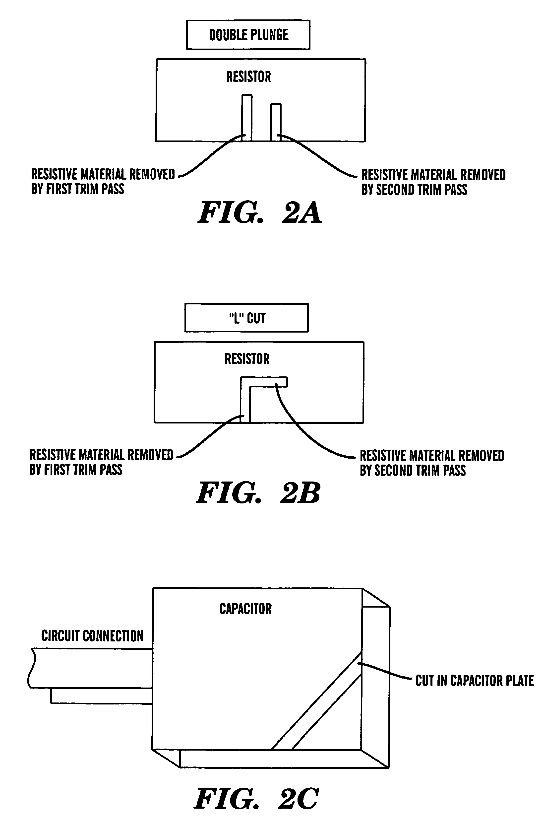
In case 2 or case 3, certain somewhat optimized trimming process factors for mitigating drift might have been selected by chance. For example, if there was some other reason to select a particular cut type, that cut might provide some optimization. However, even if this were the case, additional speed or yield improvements may still be achievable by selecting the best trim type or by optimizing another trimming process factor, such as the heat input by the laser beam to the element during trimming, to increase the process margin.

case 5

is a particularly interesting example of an implementation in which no drift is allowed after lamination. As shown, initial indications are that untrimmed resistors have negative drift of about 4% after lamination. Laser trimmed resistors have positive, e.g. 4% to 8%, post-lamination drift. Thus, by choosing the correct trimming parameters the final drift can be reduced to substantially 0%.

It will be recognized that the trimming may be performed in multiple phases. That is, all passive elements may first be subjected to a rough trimming and then be subjected to a fine trimming after the rough trimmed elements have cooled.

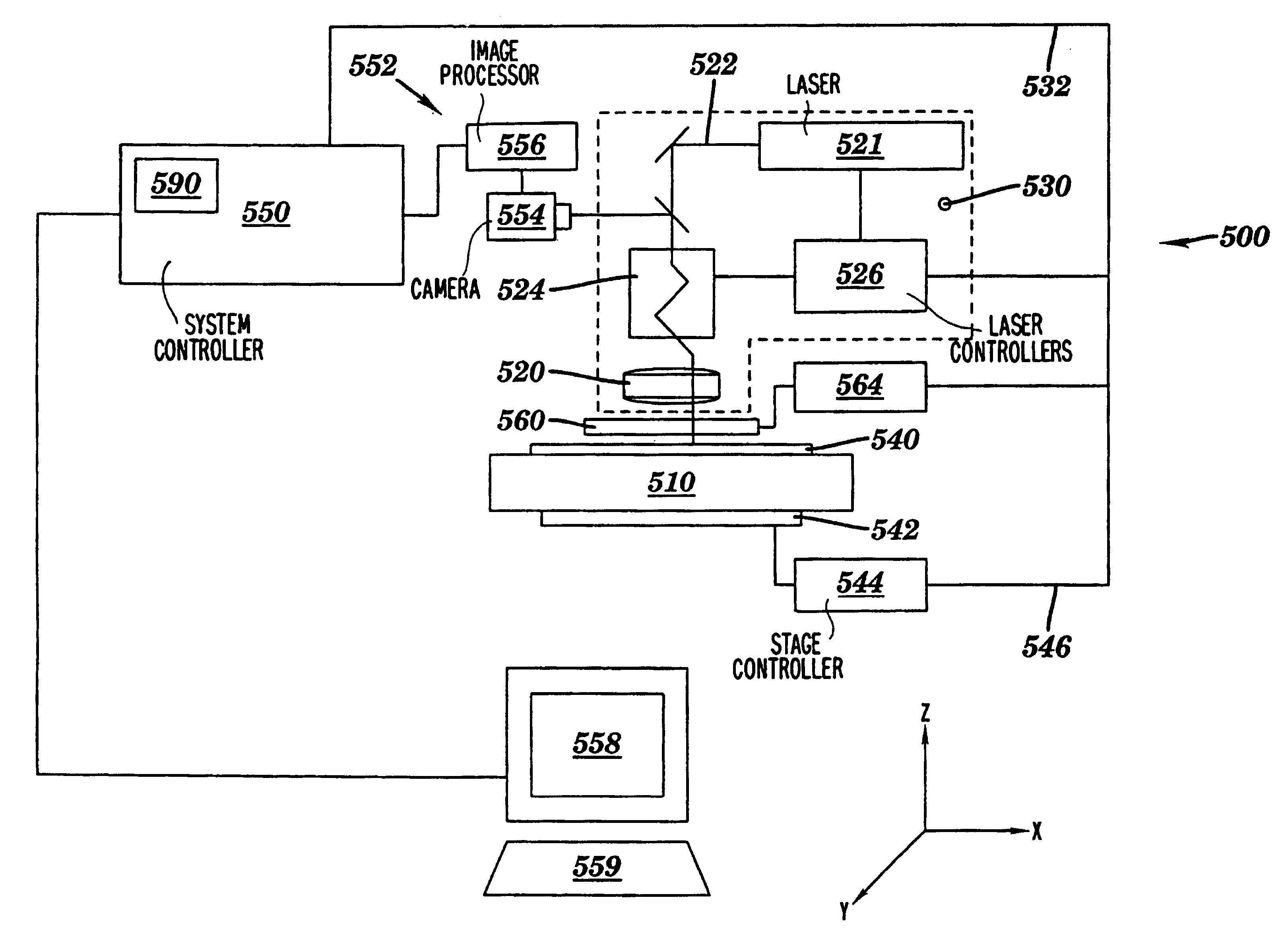
Following determination of trim (cut) speed (bite size, spot size, and repetition rate) in step 1615, operations continue with FIG. 17. In step 1701 the position of the element in relation to the any conductors (copper traces) is determined. Typically this is done by doing a global alignment (3 or 4 point alignment) to determine where the conductors are located, and...


PUM

PropertyMeasurementUnit
wavelengthaaaaaaaaaa
thicknessaaaaaaaaaa
temperatureaaaaaaaaaa

Abstract

In the laser trimming of passive circuit elements such as resistors, capacitors and inductors, various trimming parameters must be selected. To select a element is compared with a target value for the parameter to determine an offset value between the measured parameter value and the target value. The relevant trim parameters are then selected based on the determined offset values.

Description

TECHNICAL FIELDThe present invention relates to trimming elements formed on a panel or other work piece. More particularly the present invention relates to trimming elements, such as resistors, capacitors or other passive circuit elements, which may be later embedded in a layer of a multi-layer work piece, such as a Printed Circuit Board (PCB).BACKGROUND ARTMaterial processing is used to adjust the performance of electronic elements by removing or otherwise affecting a portion of the material of the electronic element to change the electrical characteristics thereof. It is known to change the electrical properties of passive and some active electronic elements by removing material therefrom. Methods of removing material include applying laser energy for vaporizing a portion of the material, applying laser energy for ablative removal of the material and applying laser energy to affect a photochemical reaction for removing and / or otherwise altering an electrical performance characteri...

Claims


Application Information

Patent Timeline
Patent Type & Authority Patents(United States)
IPC IPC(8): B23K26/00H01C17/22H01C17/242H05K1/16
CPCB23K26/0003H01C17/242H05K1/16B23K26/351
Inventor NAUMOV, ANDREIKITAI, ANTONMILLER, IAN
Owner ELECTRO SCI IND INC
Why Eureka
Try Eureka