Semiconductor device having superior resistance to moisture

Inactive Publication Date: 2005-04-05
RENESAS ELECTRONICS CORP
View PDF11 Cites 37 Cited by
  • Summary
  • Abstract
  • Description
  • Claims
  • Application Information

AI Technical Summary

Benefits of technology

It is an object of the present invention to provide a semiconductor device having a seal rin

Problems solved by technology

A major issue in the fabrication of semiconductor devices is the prevention of moisture in the atmosphere or during dicing from permeating the cross section of the diced chips and thereby degrading the performance of the internal devices.
Typically, when the chip is exposed to a heat cycle, stress tends to concentrate in the corners of the chip, and the corners of the chip are therefore vulnerable to cracking.
At this time, in a semiconductor chip in which seal ring 2 is formed in the above-described simple rectangular shape, there is a potential for cracking to occur in the

Method used


Image

  • Semiconductor device having superior resistance to moisture
  • Semiconductor device having superior resistance to moisture
  • Semiconductor device having superior resistance to moisture

Examples


Embodiment Construction

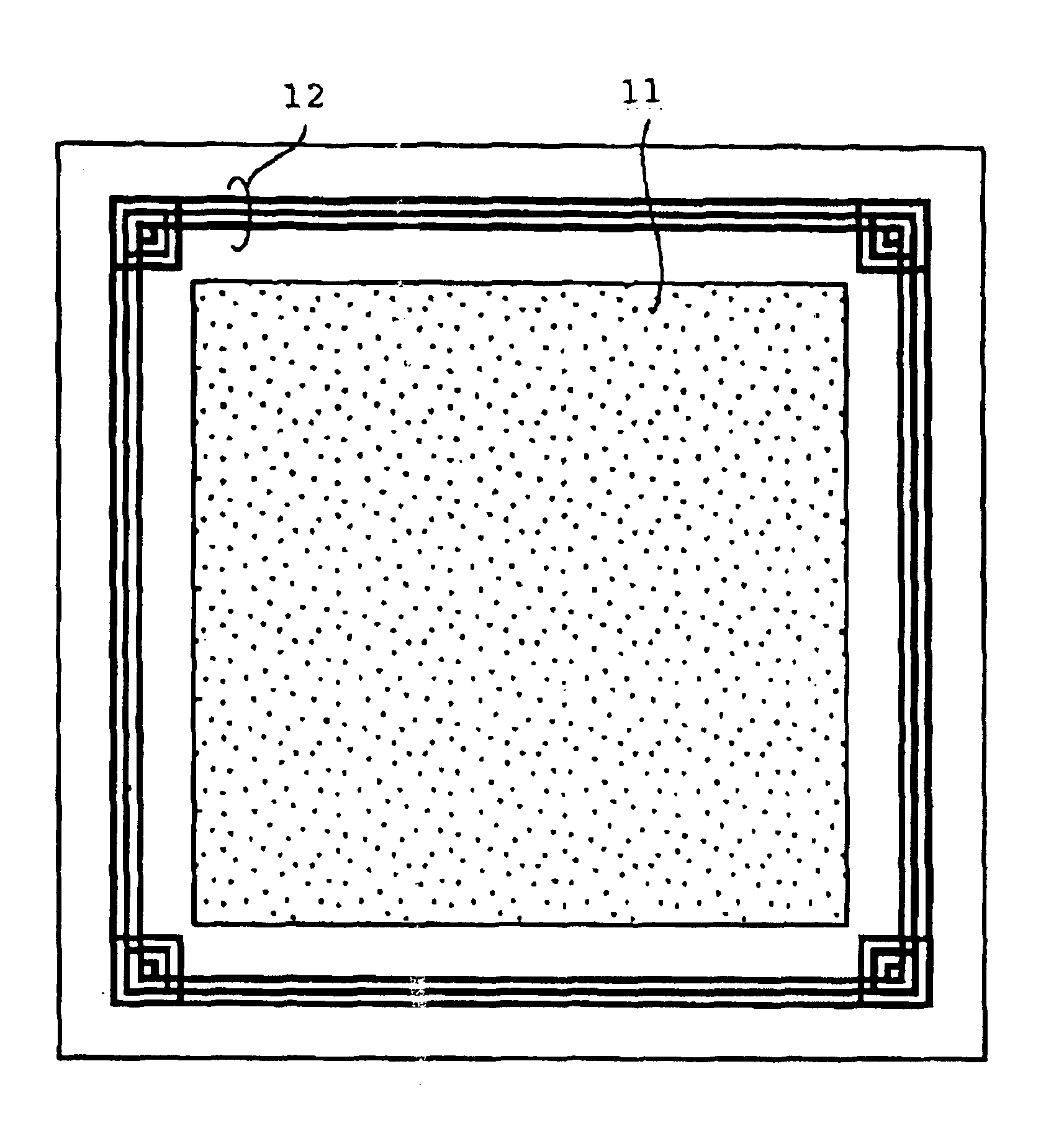
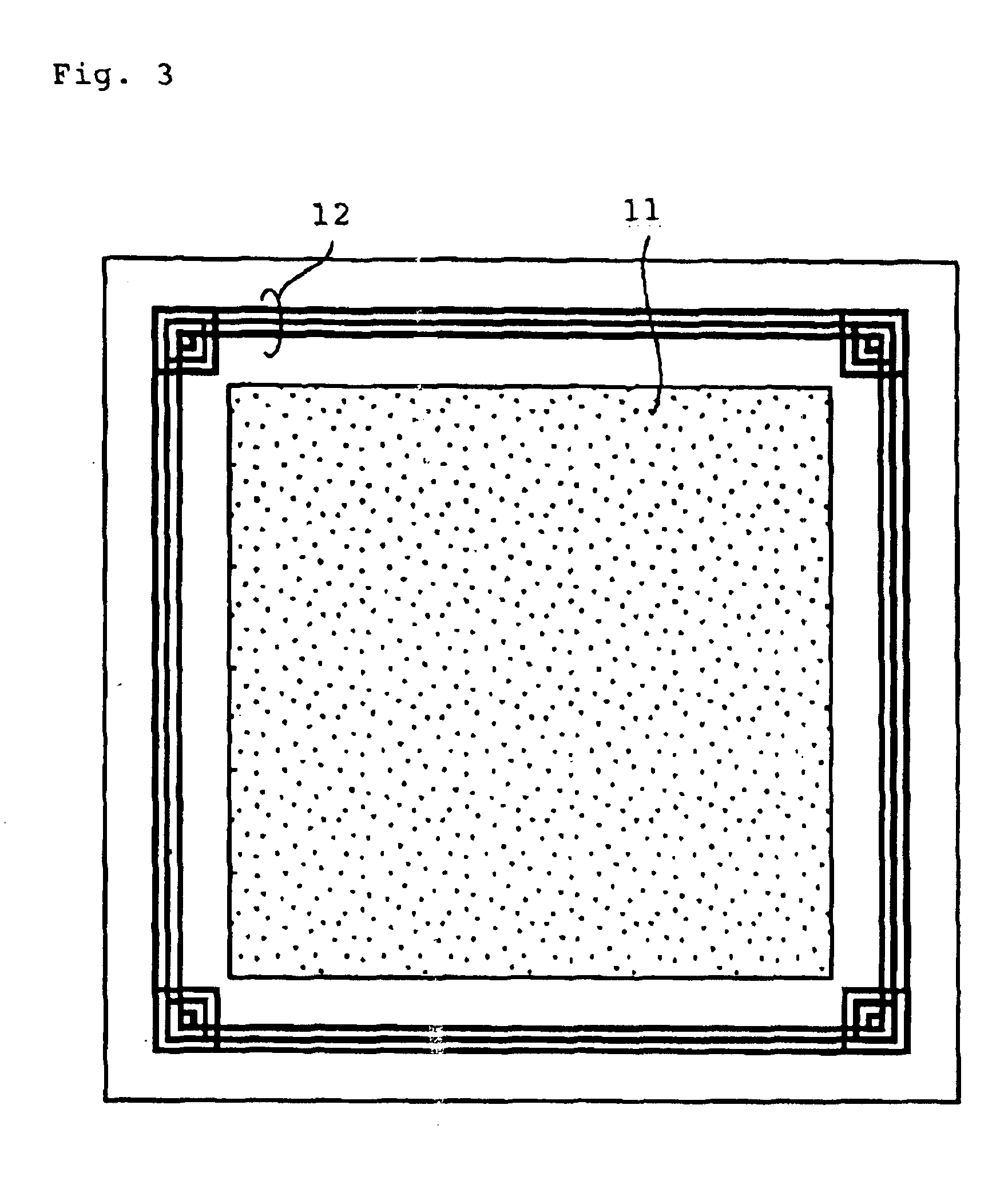
As shown in FIG. 3, in the semiconductor device of the present embodiment, circuit unit 11 is formed within the central area, and seal ring 12 is arranged so as to surround the periphery of circuit unit 11.

In the semiconductor device, dielectric film 14 that includes elements, first wiring layer dielectric film 15, first via dielectric film 16, and second wiring layer dielectric film 17 are successively stacked on silicon substrate 13, as shown in FIGS. 5 and 6. Circuit unit 11 is made up by elements, wiring, and vias (not shown in the figures) that are formed in each of these dielectric films.

Seal rings 12 are formed so as to pass through each of these dielectric films, and are composed of the same metal that is used in the wiring that is formed in each of these dielectric films. These seal rings 12 can be formed by a method that is similar to a wiring pattern formation method and are formed at the same time as the formation of the wiring pattern of the semiconductor device.

The pla...


PUM


Abstract

In a semiconductor device, a circuit unit is formed in an inside portion, and seal rings that enclose the inside portion that are composed of walls of metal layers are formed around the periphery. In the corners, the seal rings include linear parts that extend inwardly in addition to the linear parts that extend along the periphery, whereby the seal rings are formed in a planar pattern having small rectangular planar patterns in each corner.

Description

BACKGROUND OF THE INVENTION1. Field of the InventionThe present invention relates to the construction of a semiconductor device; and more particularly to the construction of walls that are impermeable to moisture (these walls being referred to hereinbelow as “seal rings”) that are provided as a single unit, that penetrate each of a plurality of interlayer dielectric films provided on a semiconductor substrate, and that are provided around the periphery of a semiconductor chip so as to enclose the inside portion of the semiconductor chip.2. Description of the Related ArtIn the process of fabricating a semiconductor device, after carrying out prescribed processes in the wafer state, the wafers are diced to chip size to obtain each semiconductor chip. A major issue in the fabrication of semiconductor devices is the prevention of moisture in the atmosphere or during dicing from permeating the cross section of the diced chips and thereby degrading the performance of the internal devices....

Claims


Application Information

Patent Timeline
IPC IPC(8): H01L23/28H01L23/00H01L23/52H01L21/3205H01L21/82H01L21/822H01L27/04
CPCH01L23/28H01L23/564H01L2924/0002H01L2924/00
Inventor MATUMOTO, AKIRAFUKASE, TADASHIIGUCHI, MANABUKOMURO, MASAHIRO
Owner RENESAS ELECTRONICS CORP
Why Eureka
Try Eureka