Triacs suffer from two major problems.
The other problem is that the device inherently has a
voltage drop associated with it, which results in significant power dissipation.
Switches based on
field effect transistors have been very successfully used for switching low-level analog signals, however, various technical difficulties have prevented their widespread acceptance for
AC power switching applications.
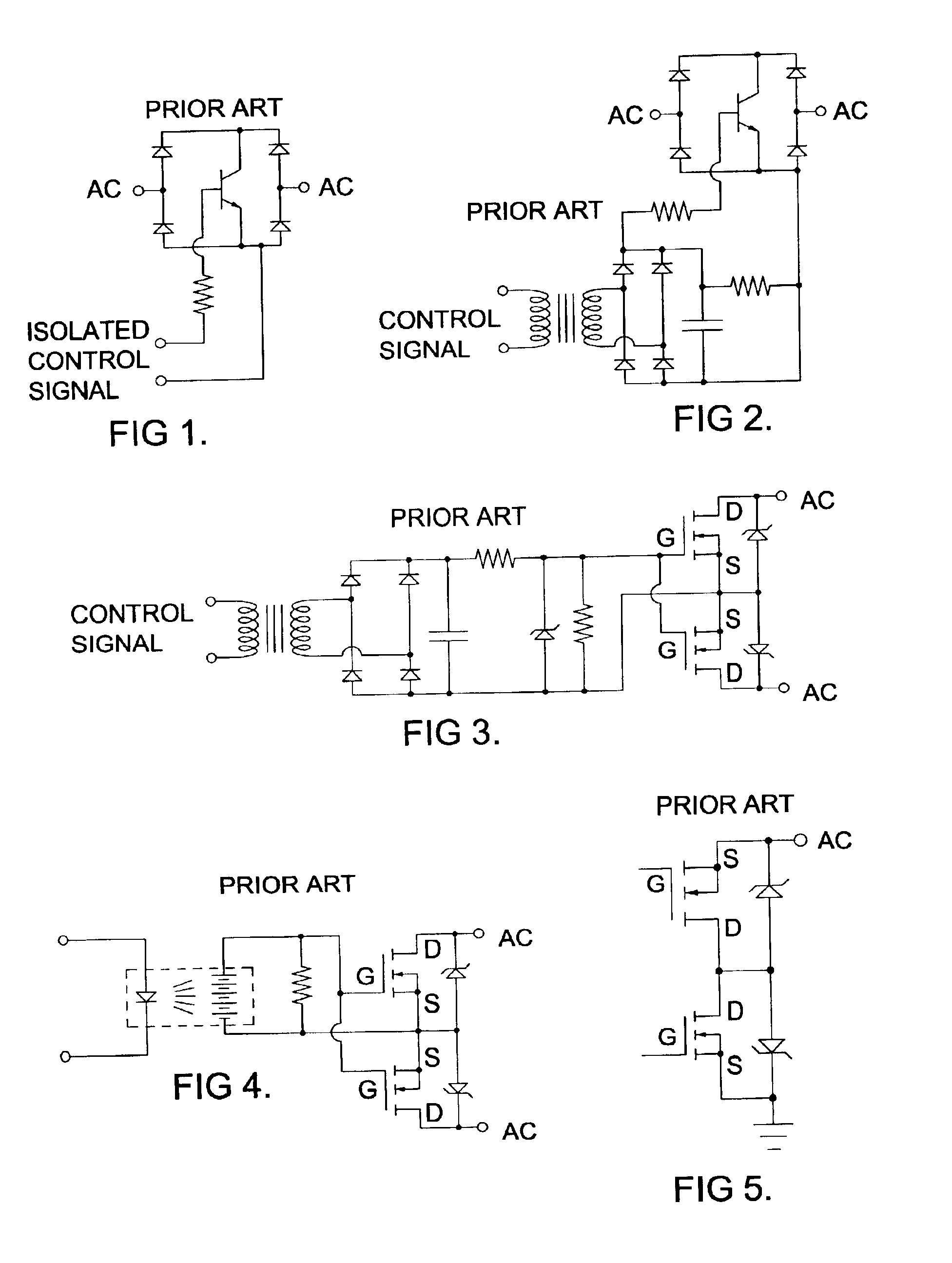
The NPN bipolar
transistor is only capable of switching on in one direction, however, the
diode bridge changes the AC at the switch terminals into DC (
direct current) going through the
transistor.
Isolation transformers do not work on DC voltages, however, if an AC voltage is provided to the
transformer input, a
diode bridge on the output of the
transformer can convert it into a
DC voltage signal suitable for driving the input of the bipolar transistor.
Still, such a switch is far from ideal due to power dissipation in the diodes and the bipolar transistor.
This is due to the inherent voltage drops in these devices.
Referring now to FIG. 3 it is shown how power dissipation can be greatly reduced through the use of field effect transistors, however, the problem of isolation between the AC voltage and the
control signal remains.
However, field effect transistors will only block voltage in one direction when in the off-state.
The prior art method of isolation presented in FIG. 3 suffers from a number of problems.
Finally, there is a loss of speed of response due to the frequency limitation of the
transformer and the rectification circuit.
The two major drawbacks of this approach are the cost of the photo-voltaic
isolator, and its
slow speed of response.
However, Huth et al do not give any details on how to drive the
field effect transistor inputs while maintaining adequate separation between the
control signal for the switch and the analog signals being switched.
In particular, it makes the circuit more complicated, it adds to the cost, and it slows down the speed of the device.
However, his circuit is only suitable for switching low level analog signals.
Any AC voltage of 120 V would subject his bipolar transistors, used as drivers, to excessive emitter-base voltages which would damage the devices.
This makes Sorchych's device unsuitable for use as a power switch in many typical applications.
The result is a circuit which is not particularly energy-efficient.
Any
AC power going through the switch must pass through one
diode having a diode drop of 0.7 Volts and one power transistor having a
voltage drop of at least 0.3 Volts resulting in an overall
voltage drop of at least 1 V. This results in a power dissipation of at least one
Watt per Amp.
In addition to the problem of high power dissipation resulting from the
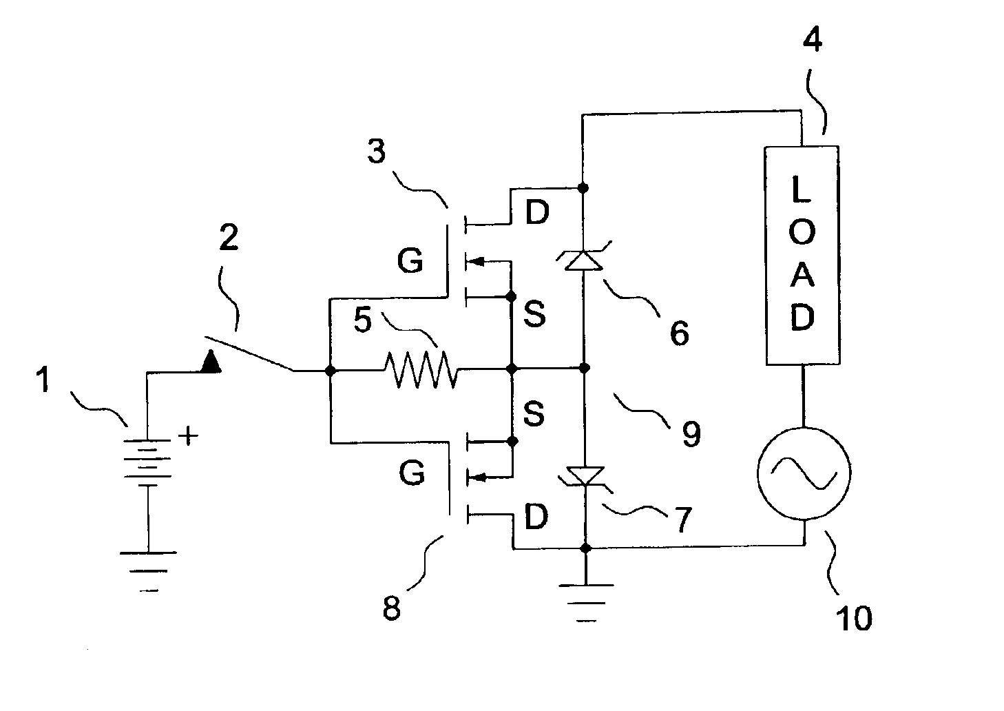
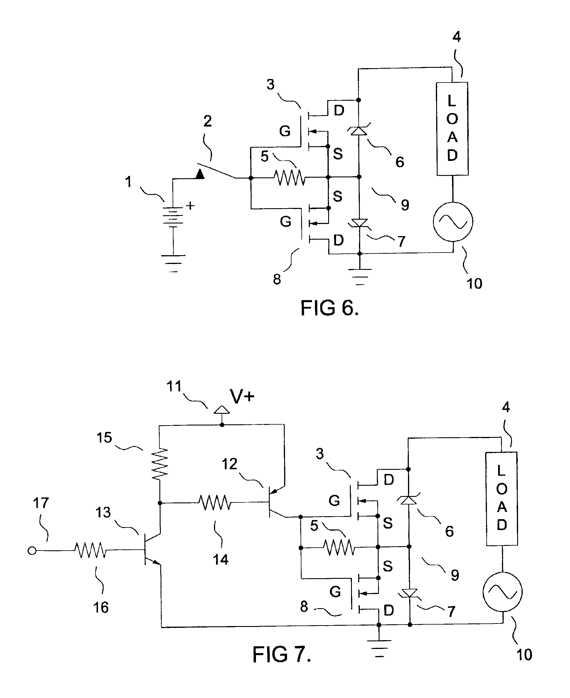
voltage drop across the insulated gate bipolar transistors and diodes in the circuit, this circuit has limited use because Laughton grounds the emitters of the insulated gate bipolar transistors.
This eliminates the need to isolate the
signal input, however, this circuit can only be used where the AC voltage is isolated.
In most cases this would require an expensive power
isolation transformer, which would of course be more costly than a signal isolation transformer.
Furthermore, this would not be a particularly energy efficient switch due to resistors in series with the field effect transistors, and the voltage drops across the thyristors.
In addition to these drawbacks the control would be limited, because once triggered, the thyristors would remain on until the next
zero crossing in the AC voltage.
The result of this is that the voltage capability of the switch is limited by the gate-source breakdown voltages of the field effect transistors which is typically 20 Volts.
This makes the circuit unsuitable for typical power applications which require substantially higher voltages.
The result of this is that the voltage capability of the switch is limited by the gate-source voltage capability of these field effect transistors.
Another problem is that the switch does not respond immediately to activating control signals, but rather waits for the next
zero crossing before turning on.
The third problem has to do with energy efficiency.
One could, of course, speed up the switch by lowering the resistance of the
resistor R1, but that would result in increased power dissipation in the
resistor due to the high-voltage AC.

