Integrated modulator and demodulator configuration

a modulator and configuration technology, applied in the field of communication, can solve the problems of significant power consumption and complex digital data, and achieve the effect of reducing circuit area, cost and power consumption

Inactive Publication Date: 2005-04-05
INTELLECTUAL VENTURES I LLC
View PDF13 Cites 21 Cited by
  • Summary
  • Abstract
  • Description
  • Claims
  • Application Information

AI Technical Summary

Benefits of technology

An integrated demodulator and decimator circuit and an integrated modulator and interpolator circuit according to embodiments of the present invention significantly reduce circuit area, cost and power consumption. The integrated demodulator and decimator circuit processes digital samples of a received signal having a predetermined intermediate frequency (IF) and that has been sampled at a sample rate based on a clock having a frequency that is four times the IF. The integrated demodulator and decimator circuit includes a selective digital sign inverter and a decimator. The selective digital sign inverter sign inverts the sign of selected digital samples according to a predetermined phase-shift pattern and outputs demodulated digital samples at the sample rate. The decimator is provided in the form of a FIR filter with a plurality of taps, where the demodulated digital samples are sequentially shifted through the filter taps at the sample rate. The decimator outputs complex digital values at half of the sample rate, where the complex digital values are derived from taps whose outputs are always either real or imaginary only. In a specific embodiment, the decimator is a symmetric half-band FIR filter with alternating zero and non-zero taps including a center tap. The complex output includes real output values based on demodulated digital samples shifted into alternate taps and corresponding imaginary output values based on demodulated digital samples shifted into the center tap.

Problems solved by technology

Encoding schemes such as OFDM result in complex digital data including real and imaginary digital samples in the transmitter.
The additional number of components and resulting large size of the circuitry had further resulted in significant power consumption.

Method used


Image

  • Integrated modulator and demodulator configuration
  • Integrated modulator and demodulator configuration
  • Integrated modulator and demodulator configuration

Examples


Embodiment Construction

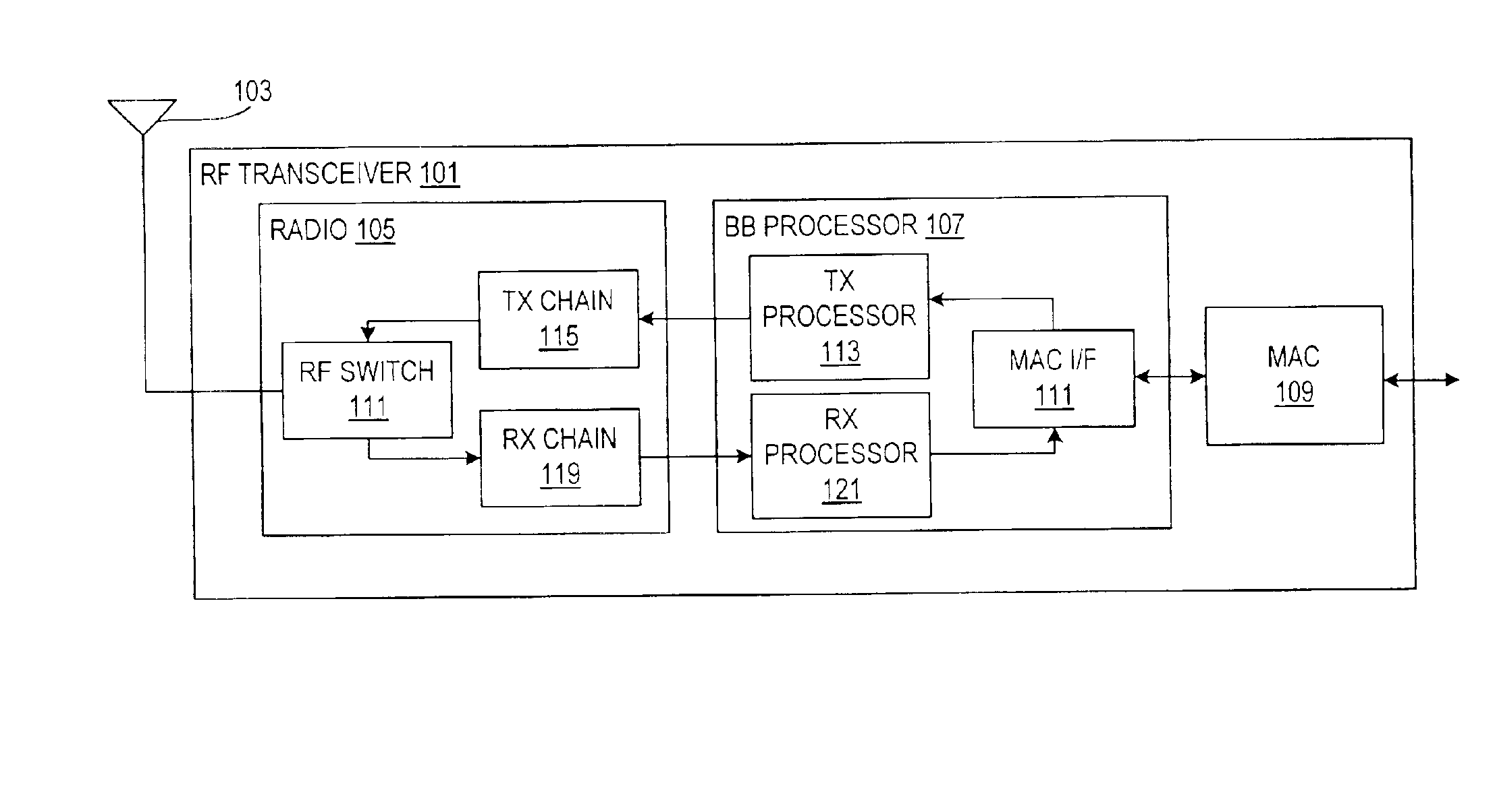
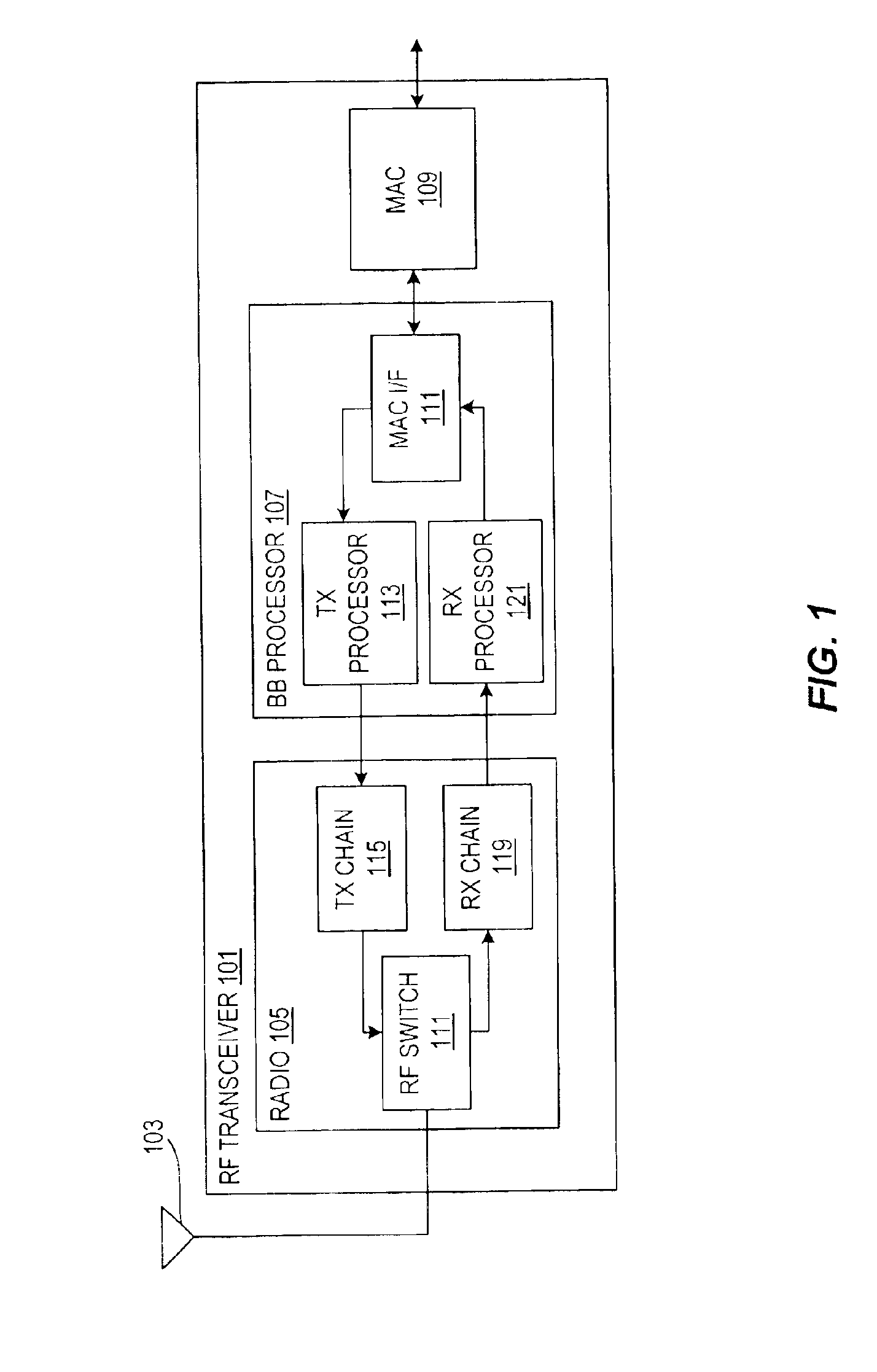
FIG. 1 is a block diagram of a wireless radio frequency (RF) transceiver 101 implemented according to an embodiment of the present invention. The transceiver 101 may be used to communicate with one or more similar wireless devices across a wireless medium, such as within a wireless local area network (WLAN) or the like. Although the present invention is illustrated for use in a WLAN device in exemplary embodiments, it is understood that the present invention is not limited to WLAN applications or even wireless applications but instead applies to any wired or wireless communication device employing modulation and demodulation functions. The transceiver 101 may be used by any type of device to incorporate wireless communication capabilities, such as a wireless access point (AP), any type of computer or computer system (e.g., personal computers, laptop computers, desktop computers, etc.,), printing devices including any type of printer technology, personal digital assistants (PDAs) or ...


PUM


Abstract

An integrated demodulator and decimator circuit including a selective digital sign inverter and a decimator. The sign inverter negates selected digital samples based on Weaver demodulation and outputs demodulated digital samples at a sample rate. The decimator is a symmetric half-band FIR filter, where the demodulated digital samples are sequentially shifted through filter taps at the sample rate. The decimator outputs real output values based on digital samples shifted into alternate taps and imaginary output values based on digital samples shifted into the center tap. An integrated modulator and interpolator circuit includes a symmetric half-band FIR filter interpolator and a digital sign inverter. The interpolator includes two polyphase filters and a multiplexer. A first polyphase filter filters real digital samples and a second filters imaginary digital samples. The multiplexer provides interpolated digital samples at four times the sample rate. The digital sign inverter negates selected digital samples according to Weaver modulation.

Description

FIELD OF THE INVENTIONThe present invention relates to communications, and more particularly to an integrated configuration of a modulator and demodulator in a baseband processor of a communication device, such as a wireless RF transceiver.BACKGROUND OF THE INVENTIONModulation is the process of encoding information onto a bandpass signal for purposes of transmission via a selected medium. Many modulation techniques are known for encoding data, including single-carrier and multi-carrier methods, where the particular method chosen depends upon the application and, the selected medium of transmission. One such multi-carrier method used for wireless communications is orthogonal frequency division multiplexing (OFDM). For example, the Institute of Electrical and Electronics Engineers, Inc. (IEEE) 802.11a standard defines multiple data rates in the 5 Gigahertz (GHz) frequency band employing orthogonal frequency division multiplexing (OFDM) for use with Wireless Local Area Networks (WLANs)...

Claims


Application Information

Patent Timeline
Patent Type & Authority Patents(United States)
IPC IPC(8): H03D3/00H03C3/00H03H17/06H03C3/40
CPCH03C3/40H03D3/006H03H17/0657H03H17/0664H03H17/0275H03H2218/04
Inventor WEBSTER, MARK A.PONTON, KENT A.CHIUCHIOLO, JR., PAUL J.
Owner INTELLECTUAL VENTURES I LLC
Why Eureka
Try Eureka