Image display

a technology of image display and display panel, applied in the field of image display, can solve the problems of difficult to achieve multi-level illumination, difficult to minimize the characteristic variation among devices, and difficult to provide an image display capable of multi-level illumination

Inactive Publication Date: 2005-04-05
SAMSUNG DISPLAY CO LTD +1
View PDF7 Cites 91 Cited by
  • Summary
  • Abstract
  • Description
  • Claims
  • Application Information

AI Technical Summary

Benefits of technology

The problem of this invention can also be solved by an image display which has a display area made up of a plurality of pixels and a signal line for feeding a display signal voltage to the pixels, the image display comprising, in at least one of the plurality of pixels: a memory means for storing the display signal voltage entered from the signal line to the pixel; a pixel turn-on period decision means for determining an ON period and an OFF period for an image output in the pixel according to the display signal voltage; and a pixel drive means for repeating an ON operation of the image output a plurality of times in one frame.

Problems solved by technology

With the conventional technologies described above, it is difficult to provide an image display which is capable of multi-level illumination and has a minimal pixel-to-pixel display characteristic variation.
In the first conventional technology described with reference to FIG. 16, the multi-level illumination is difficult to achieve.
Particularly when a large number of TFTs are built into, for example, a display area consisting of pixels, it is very difficult to minimize characteristic variations among devices.
In a half-tone image, the luminance non-uniformity of such a magnitude cannot be tolerated.
To avoid this luminance variation, the signal voltage to be entered needs to be limited to two values, on and off, which in turn makes the multi-level illumination including half-tone illumination difficult.
TFTs generally have large variations as described above and, particularly when a large number of TFTs are built into, for example, a display area consisting of pixels, it is very difficult to minimize characteristic variations among devices.
Therefore, even with this conventional technology, it is difficult to sufficiently minimize the illumination characteristic variation among pixels due to such a luminance non-uniformity.
In that case, the characteristic variation of the low-temperature polysilicon TFTs in turn results in a variation in the pulse width modulation, which is an output of the “PWM signal conversion circuit.” A second problem is that, in the conventionally known “PWM display method,” an image degradation is caused by “pseudo-profiling noise.” This is a phenomenon observed in a plasma display in which if the display period shifts to one side of a frame in terms of time, profiling noise appears in a video image.
It is, however, not realistic to realize such a sophisticated signal processing function with the “PWM signal conversion circuit” built into each pixel.

Method used


Image

  • Image display
  • Image display
  • Image display

Examples


first embodiment

(First Embodiment)

A first embodiment of the present invention will be described by referring to FIGS. 1 to 8.

First, an overall configuration of this embodiment will be explained by referring to FIG. 1.

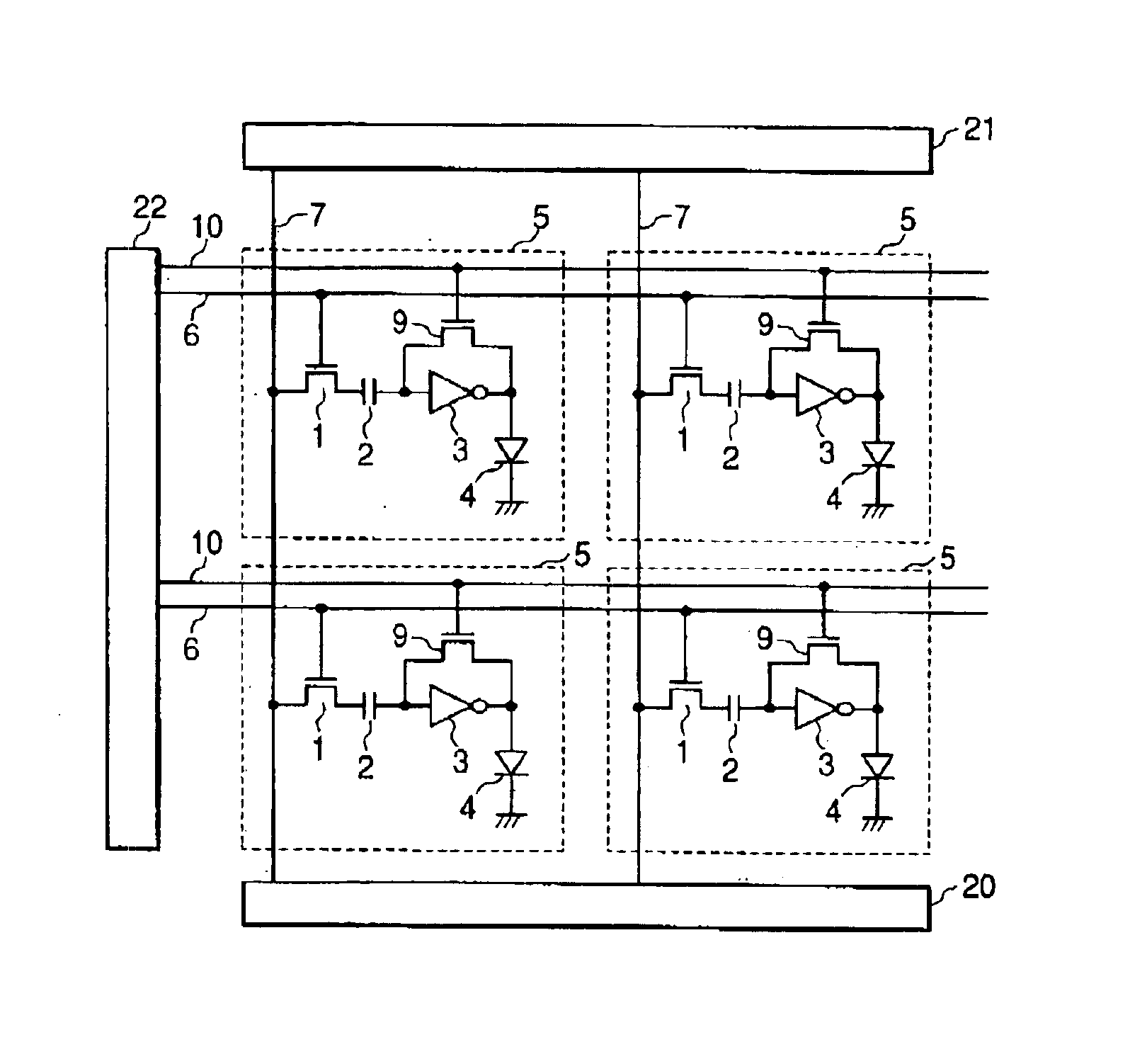
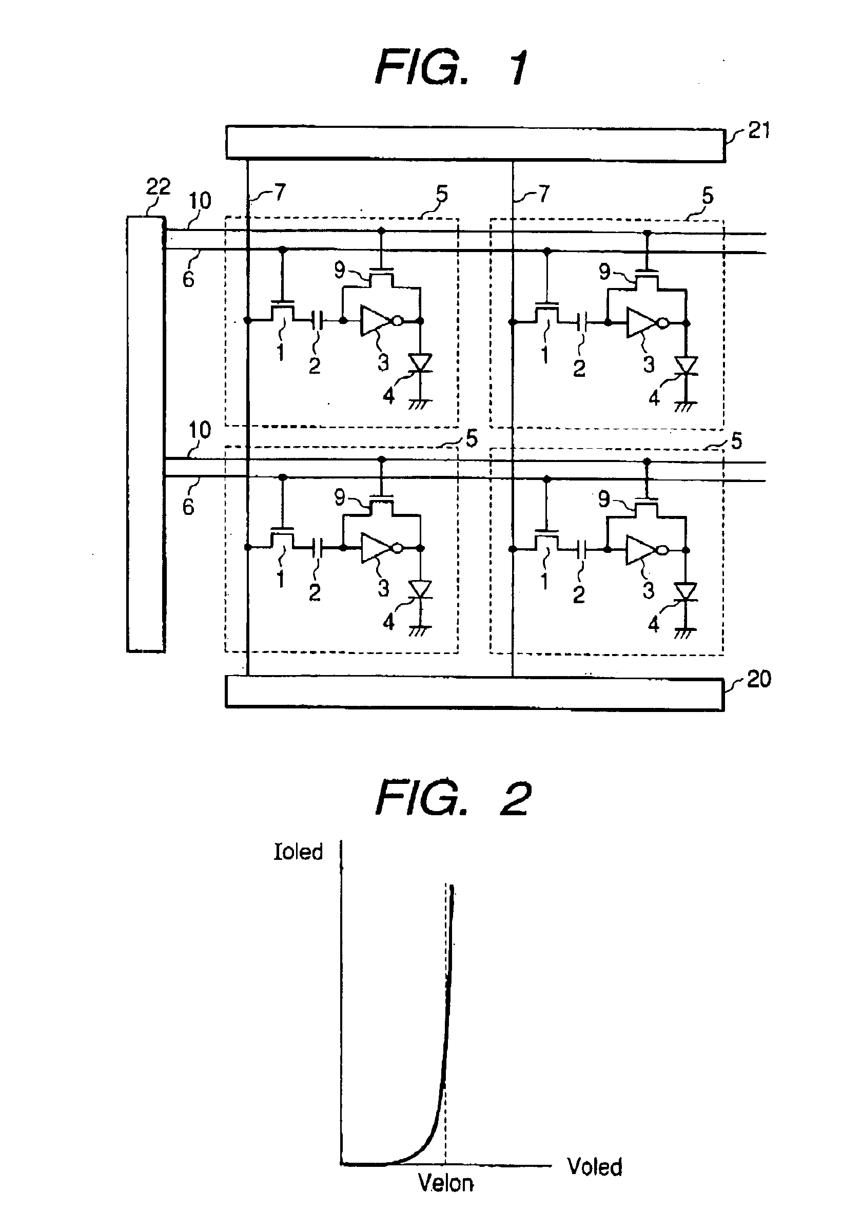
FIG. 1 shows a configuration of an organic light emitting diode (OLED) display panel of this embodiment. Pixels 5 each having an OLED 4 as a pixel light emitting device are arranged in matrix in a display area. The pixels 5 are connected to predetermined drive circuits through gate lines 6, signal lines 7 and reset lines 10. The gate lines 6 and reset lines 10 are connected to a gate drive circuit 22, and the signal lines are connected to a signal drive circuit 21 and a triangular wave (triangular pattern) input circuit 20. The pixels 5, gate drive circuit 22, signal drive circuit 21 and triangular wave input circuit 20 are all formed from polysilicon TFTs on a glass substrate. In each pixel 5, the signal line 7 is connected through an input TFT 1 to one end of a storage capacitor 2, t...

second embodiment

(Second Embodiment)

A second embodiment of the present invention will be described by referring to FIG. 9.

The configuration and operation of this embodiment are basically similar to those of the first embodiment, except that the operation waveform of the signal line 7 differs from that of the first embodiment shown in FIG. 5. Thus, the descriptions of the configuration and operation of this embodiment are omitted here and only the operation waveform of the signal line 7, which is the feature of this embodiment, will be explained.

FIG. 9 shows the operation waveform of the signal line 7 in the second embodiment. In the first embodiment, during the driving periods the same pixel driving voltage sweep waveform is repeated for each horizontal scanning period. In the second embodiment, however, the pixel driving voltage sweep waveform is divided into three parts and three horizontal scanning periods combine to form one cycle of the triangular wave (triangular pattern).

This arrangement in t...

third embodiment

(Third Embodiment)

Now, a third embodiment of the present invention will be described by referring to FIG. 10.

The configuration and operation of this embodiment are basically similar to those of the first embodiment, except that the operation waveform of the signal line 7 differs from that of the first embodiment shown in FIG. 5. Thus, the descriptions of the configuration and operation of this embodiment are omitted here and only the operation waveform of the signal line 7, which is the feature of this embodiment, will be explained.

FIG. 10 shows the operation waveform of the signal line 7 in the third embodiment. In the first embodiment, the pixel driving voltage sweep waveform during the driving period is a continuously changing triangular wave. In the third embodiment, the writing signal is a 4-level (2-bit) illumination signal and the pixel driving voltage sweep waveform is also a 4-level stepped waveform. It should be noted here that each of the four voltage levels of the 4-leve...


PUM

PropertyMeasurementUnit
threshold voltageaaaaaaaaaa
voltageaaaaaaaaaa
capacitanceaaaaaaaaaa

Abstract

An image display capable of multilevel display and having a minimal pixel-to-pixel display characteristic variation. The image display having a display area of a plurality of pixels and a signal line for feeding a display signal voltage to the pixels, comprises, in at least one of the plurality of pixels: a memory for storing the display signal voltage entered from the signal line to the pixel; a pixel turn-on period decision section for determining an ON period and an OFF period for an image output in the pixel according to the display signal voltage; and a pixel driver for repeating an ON operation of the image output a plurality of times in one frame.

Description

BACKGROUND OF THE INVENTIONThe present invention relates to an image display capable of multilevel illumination and more specifically to an image display with a sufficiently small display characteristic variation among pixels.Referring to FIGS. 16, 17 and 18, two conventional technologies will be described.FIG. 16 shows a configuration of a light emitting display device. Pixels 205 each having an organic electroluminescent device 204 as a pixel light emitting device are arranged in matrix in a display area and are connected to external drive circuits via gate lines 206, source lines 207 and power supply lines 208. In each pixel 205, the source line 207 is connected to a gate of a power TFT 203 and one end of a storage capacitor 202 through a logic TFT (thin-film transistor) 201, with one end of the power TFT 203 and the other end of the storage capacitor 202 connected in common to the power supply line 208. The other end of the power TFT 203 is connected to a common power supply ter...

Claims


Application Information

Patent Timeline
Patent Type & Authority Patents(United States)
IPC IPC(8): G09F9/33G09G3/30G09F9/30G09G3/00G09G3/20G09G3/32H01L33/00H05B33/02H05B33/12H05B33/08G02F1/136G09G3/36H01L27/32H01L33/26H01L33/44H01L51/50H05B44/00
CPCG09G3/3258G09G3/2014G09G2300/0417G09G2300/0842G09G2320/0233G09G2300/0861G09G2310/0259G09G2310/066G09G2300/0852G09G3/30
Inventor AKIMOTO, HAJIMENISHITANI, SHIGEYUKIKOMURA, SHINICHISATO, TOSHIHIROKAGEYAMA, HIROSHISHIMIZU, YOSHITERU
Owner SAMSUNG DISPLAY CO LTD
Why Eureka
Try Eureka