Decode path gated low active power SRAM

a low active power, path gate technology, applied in static storage, information storage, digital storage, etc., can solve the problems of imposing stringent design constraints on active power, power consumption caused primarily by logic state switching, etc., to reduce switching power

Inactive Publication Date: 2005-04-05
GLOBALFOUNDRIES US INC
View PDF3 Cites 24 Cited by
  • Summary
  • Abstract
  • Description
  • Claims
  • Application Information

AI Technical Summary

Benefits of technology

Preferably, an address gated pulse schema is implemented to synchronize and restrict switching activity spatially and temporally to only regions of a memory array that are being accessed, and for limited periods of time just sufficient to generate signals for read or write

Problems solved by technology

As SOCs (system-on-a-chip) become more highly integrated with millions of devices being packed into a single SOC, power consumption is a critical design consideration due to the increasing gap between the energy required by portable computation/communication devices and the energy supplied by the battery.
Traditionally, in a CMOS device, power consumption is caused primarily from the switching of logic states.
Single-cycle SRAM caches that are employed for fast, low cost wireless DSP applications (such as 3G cell phones) impose stringent design constraints on active power.
With increases in the spread of Vt (threshold voltage) fluctuations that exist in cell and sense amplifier transistors, delay variability of the bit path increases dramatically at low operating voltages, requiring larger margins for evaluate periods of the SRAM cell and sense amplifier

Method used


Image

  • Decode path gated low active power SRAM
  • Decode path gated low active power SRAM
  • Decode path gated low active power SRAM

Examples


Embodiment Construction

Preferred embodiments of the present invention will be described hereinbelow with reference to the accompanying drawings. In the following description, a detailed description of well-known memory functions and architectures will not be provided to avoid obscuring the invention in unnecessary detail.

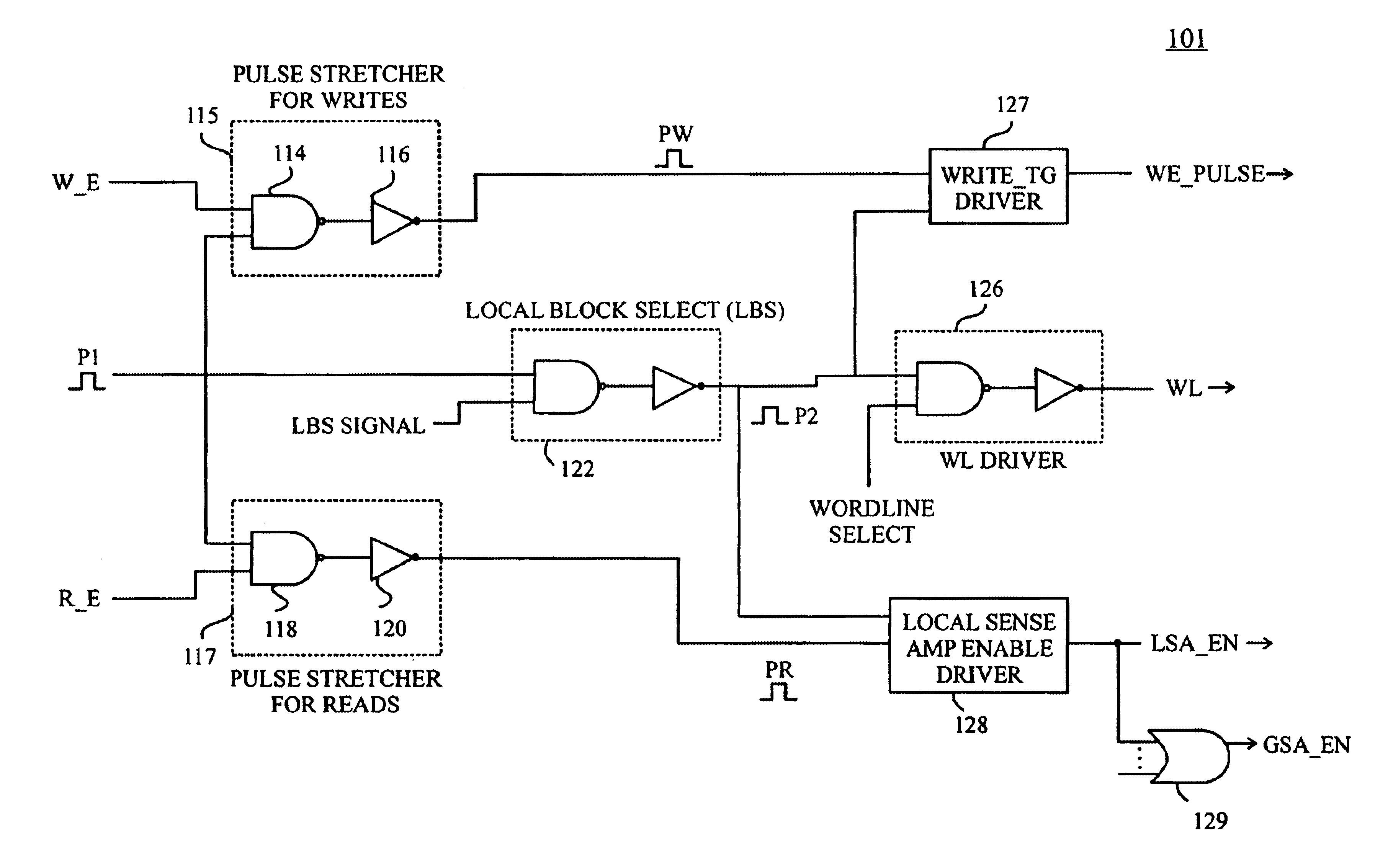
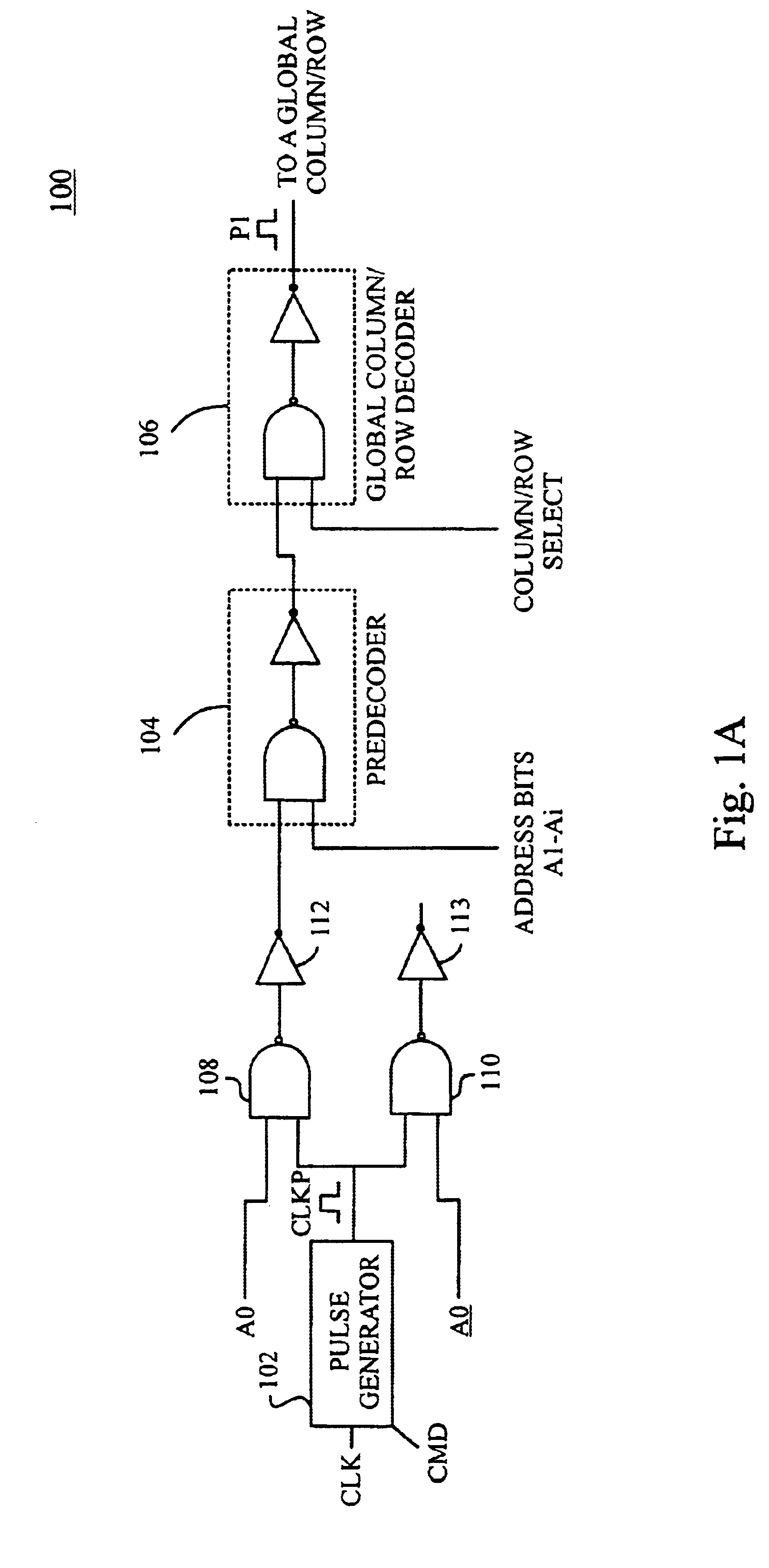
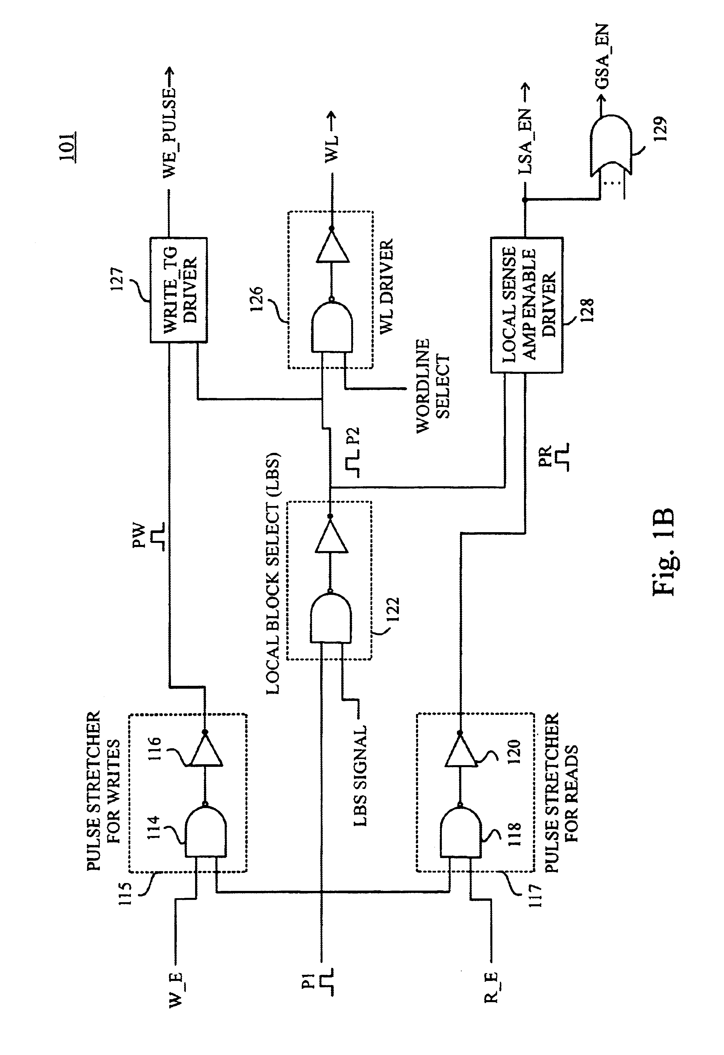
The present invention is directed to circuits and methods that provide timing and control for memory access operations in memory devices such as SRAM devices, for example, by propagating a control pulse along a decode path from which a sequence of control pulses are generated at points in the decode path to synchronize activation of wordlines and sense amplifiers and precharge / equalization of bit lines. Advantageously, circuits and methods according to the present invention enable a dramatic reduction in the switching power dissipation of conventional synchronous (clocked) SRAM arrays without incurring the performance penalties that arise from eliminating the clock distribution network in...


PUM


Abstract

Circuits and methods for controlling data access operations in memory devices such as SRAM (static random access memory) devices. The circuits and methods provide timing and control for memory access operations by propagating a control pulse along a decode path from which a sequence of control pulses are generated at points in the decode path to synchronize activation of wordlines and sense amplifiers and precharge/equalization of bit lines. Preferably, an address gated pulse schema is implemented to synchronize and restrict switching activity spatially and temporally to only regions of a memory array that are being accessed, and for limited periods of time just sufficient to generate signals for read or write operations. Advantageously, the circuits and methods enable SRAM cell delays to track CMOS gate delays more closely at low voltages and reduce switching power by restricting switching transitions only to the regions of memory that are accessed.

Description

TECHNICAL FIELD OF THE INVENTIONThe present invention relates generally circuits and methods for controlling data access operations in SRAM (static random access memory) devices. More specifically, the present invention relates to circuits and methods for controlling memory access operations by propagating a control pulse along a decode path from which a sequence of control pulses are generated at points in the decode path to synchronize activation of wordlines and sense amplifiers and precharge / equalization of bit lines.BACKGROUNDAs SOCs (system-on-a-chip) become more highly integrated with millions of devices being packed into a single SOC, power consumption is a critical design consideration due to the increasing gap between the energy required by portable computation / communication devices and the energy supplied by the battery. Traditionally, in a CMOS device, power consumption is caused primarily from the switching of logic states. In particular, the switching power is expresse...

Claims


Application Information

Patent Timeline
IPC IPC(8): G11C8/18G11C8/00G11C8/08G11C11/413
CPCG11C8/08G11C11/413G11C8/18
Inventor BHAVNAGARWALA, AZEEZKOSONOCKY, STEPHEN V.
Owner GLOBALFOUNDRIES US INC
Why Eureka
Try Eureka