Memory system having point-to-point bus configuration

a memory system and configuration technology, applied in the field of memory system configuration, can solve the problems of signal reflection, configuration has a fundamental limit in increasing the data transmission rate, and the overall data transmission rate of the system is limited

Inactive Publication Date: 2005-04-05
SAMSUNG ELECTRONICS CO LTD
View PDF17 Cites 92 Cited by
  • Summary
  • Abstract
  • Description
  • Claims
  • Application Information

AI Technical Summary

Problems solved by technology

A stub load behaves on a transmission line as a discontinuous point, which results in signal reflection.
Signal reflection due to the stub load deteriorates signal integrity, thereby limiting the overall data transmission rate of the system.
However this configuration has a fundamental limit in increasing the data transmission rate because, although the adverse effects of the stub load are mitigated, the load is still included in the configuration.
However since two pins are required for each signal, the resulting number of module pins is double the number required by the stub bus structure, which increases system costs.
Moreover, the loading of a signal line increases as the number of modules increases, which limits the maximum operable data transmission rate.

Method used


Image

  • Memory system having point-to-point bus configuration
  • Memory system having point-to-point bus configuration
  • Memory system having point-to-point bus configuration

Examples


Embodiment Construction

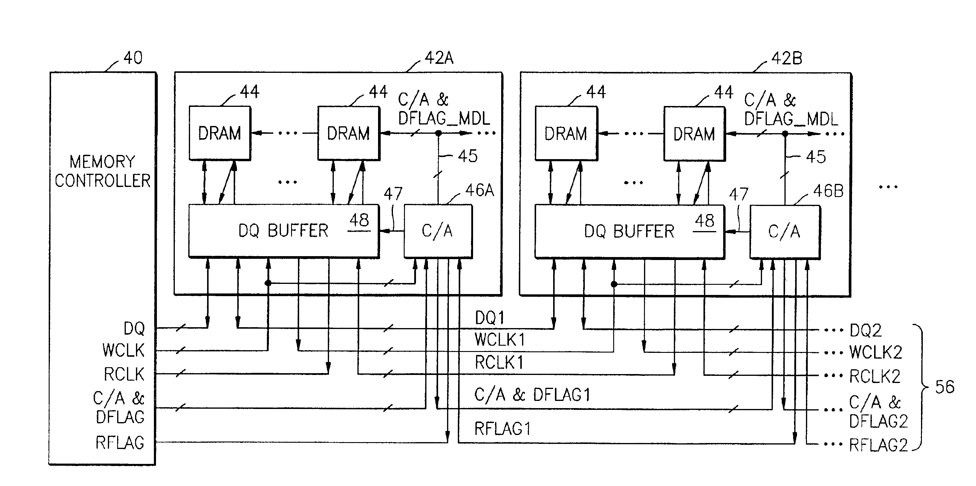
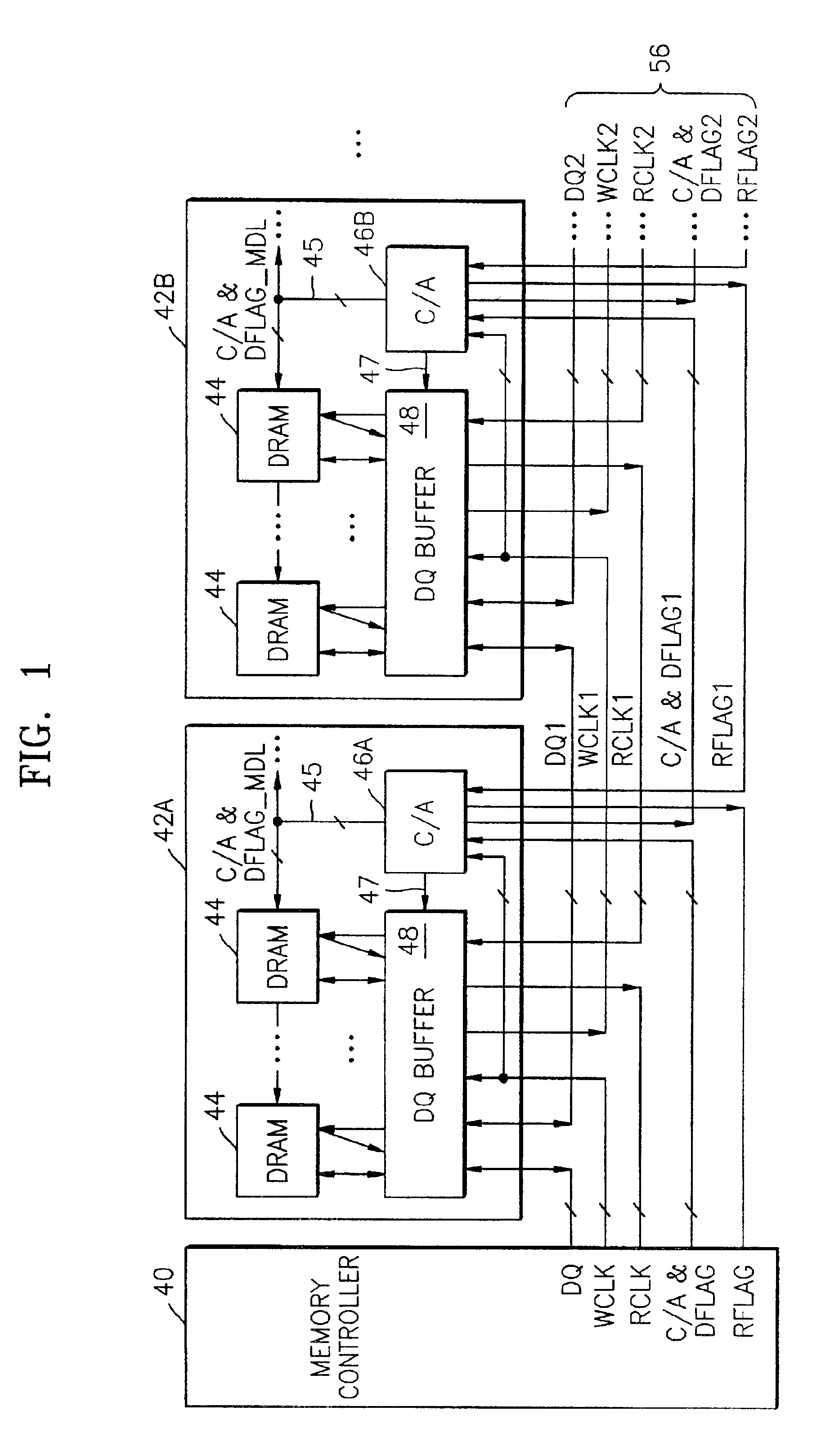
FIG. 1 is a schematic block diagram of a memory system according to the present invention. The memory system includes a memory controller 40, a plurality of memory modules 42A, 42B. A number of signal lines 56, for example mounted on a motherboard transfer signals between the memory controller 40 and the various modules 42A, 42B.

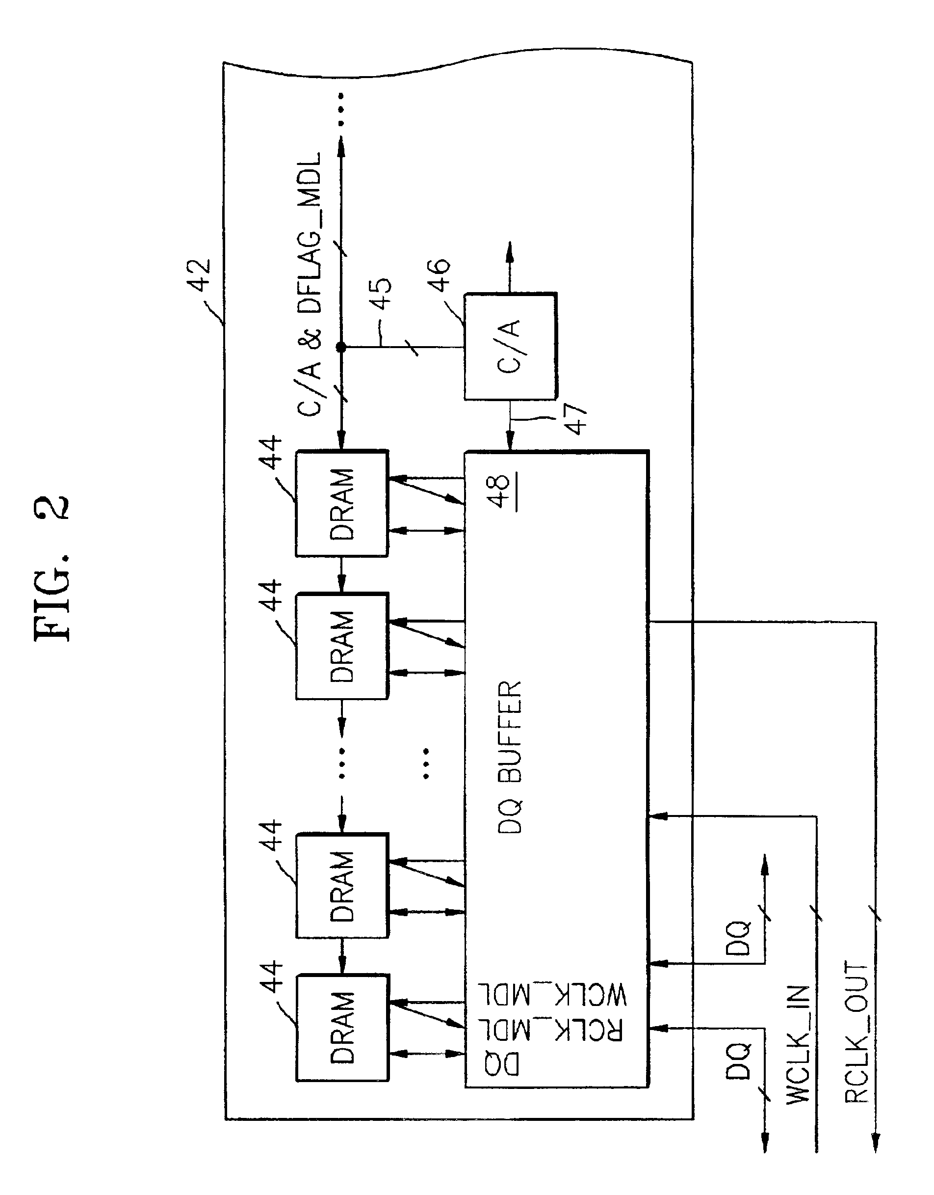
Each memory module 42A, 42B includes a data buffer 48, a command / address signal buffer 46, and a plurality of memory devices 44. In one example, the memory devices 44 may comprise dynamic random access memory (DRAM) devices. The data buffer 48 manages the buffering of data signals on the data bus DQ, and transfers the data in response to a write clock signal WCLK and a read clock signal RCLK, among others. The command / address buffer 46 manages the buffering of command signals, address signals, and flag signals, and controls the data buffer 48 and the memory devices 44 in accordance with the command, address, and flag signals. During a write operation, the da...


PUM


Abstract

A clocking system and method in a point-to-point bus configuration overcomes the limitations of conventional approaches. In one embodiment, the present invention ensures the same phase relationship for the write clock in the write direction for all data transfers between modules, and similarly the same phase relationship for the read clock in the read direction for all data transfers between modules, regardless of module location. In another embodiment, on a given module, all transfers of data between a data buffer and a memory device in both read and write directions are clocked by a read clock signal and a write clock signal that have the same phase relationship and have the same propagation delay as the data bus between the buffer and the memory device.

Description

BACKGROUND OF THE INVENTIONMemory systems are often times arranged in a stub architecture. In such an architecture, memory modules are arranged in parallel as stubs along a common data bus, control / address bus, and clock bus. In order to increase data transmission rates in a memory system having a stub bus architecture, careful control over signal integrity is necessary; signal integrity in turn being affected by the stub load. A stub load behaves on a transmission line as a discontinuous point, which results in signal reflection. Signal reflection due to the stub load deteriorates signal integrity, thereby limiting the overall data transmission rate of the system.Attempts have been made to suppress the detrimental affect of a stub load by configuring the stub bus according to a stub-series-terminated-logic (SSTL) architecture. However this configuration has a fundamental limit in increasing the data transmission rate because, although the adverse effects of the stub load are mitiga...

Claims


Application Information

Patent Timeline
Patent Type & Authority Patents(United States)
IPC IPC(8): G06F13/42G06F13/16G06F12/00
CPCG06F13/4273G06F12/00
Inventor YOO, CHANG-SIKKYUNG, KYE-HYUN
Owner SAMSUNG ELECTRONICS CO LTD
Why Eureka
Try Eureka