Method of forming copper wire on semiconductor device

a technology of semiconductor devices and wires, applied in the direction of semiconductor devices, electrical equipment, basic electric elements, etc., can solve the problems of poor etching properties of copper, the method of forming a copper wire on a semiconductor device according to the wire-making process using copper and materials with low dielectric constants, and the inability to meet the requirements of the device, so as to prevent the natural oxidation of copper

Inactive Publication Date: 2005-04-12
CHUNG CHENG HLDG LLC
View PDF13 Cites 1 Cited by
  • Summary
  • Abstract
  • Description
  • Claims
  • Application Information

AI Technical Summary

Benefits of technology

Accordingly, the present invention has been made to solve the above-mentioned problems occurring in the prior art, and an object of the present invention is to provide a method of forming a copper wire on a semiconductor device that prevents the natural oxidation of copper by selectively depositing aluminum on the surface of a copper wire pad.

Problems solved by technology

However, a wire-making process using copper and materials with low dielectric constants incurs a problem as regards the very poor etching property of copper.
However, the method of forming a copper wire on a semiconductor device according to the prior art has a problem as follows.
However, the copper wire also has a drawback: the natural oxidation of copper.
Such a natural oxidation of copper is problematic in that it decreases the reliability of the copper wire itself and even deteriorates the bonding property during packaging.

Method used


Image

  • Method of forming copper wire on semiconductor device
  • Method of forming copper wire on semiconductor device
  • Method of forming copper wire on semiconductor device

Examples


Embodiment Construction

Hereinafter, a preferred embodiment of the present invention will be described with reference to the accompanying drawings. In the following description and drawings, the same reference numerals are used to designate the same or similar components, and so repetition of the description on the same or similar components will be omitted.

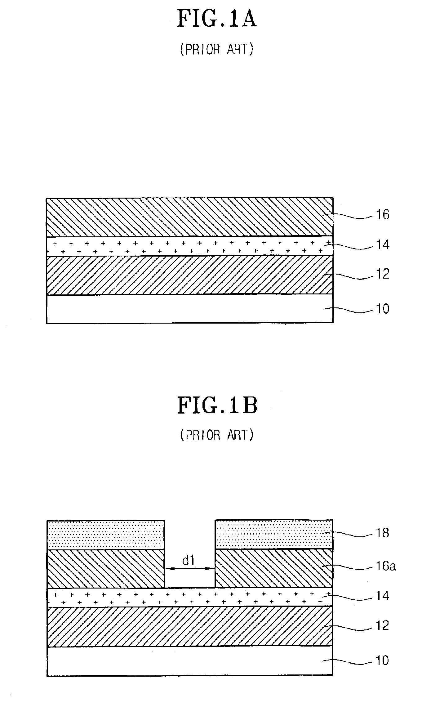
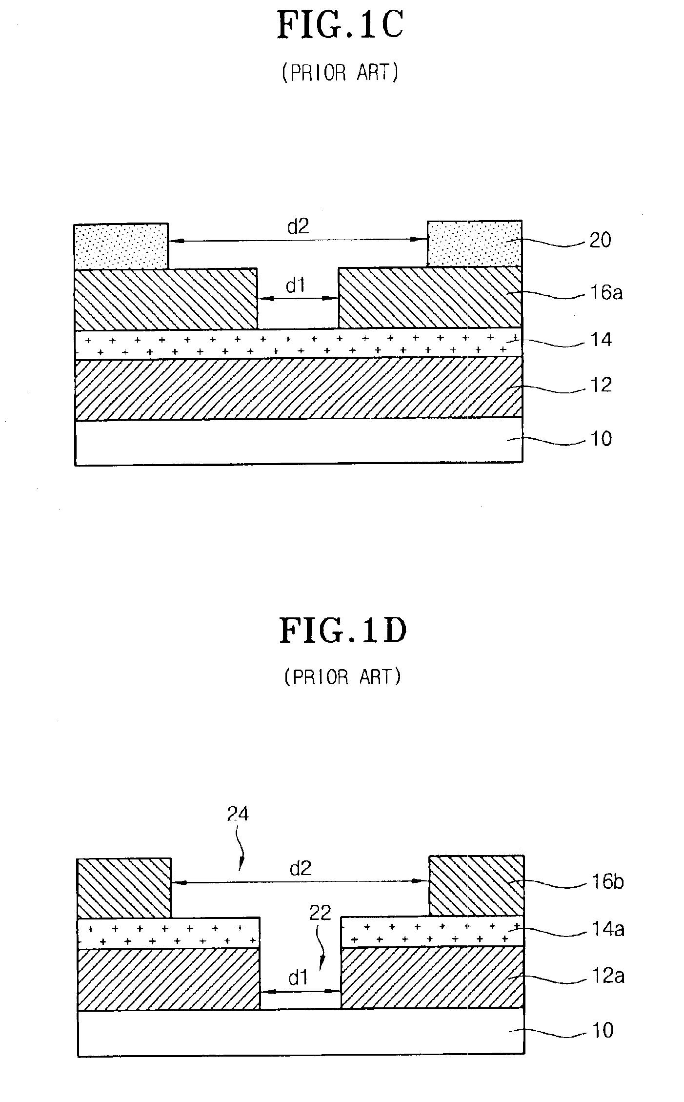
FIGS. 2a through 2e are sectional diagrams showing each process constituting a method of forming a copper wire on a semiconductor device according to the present invention.

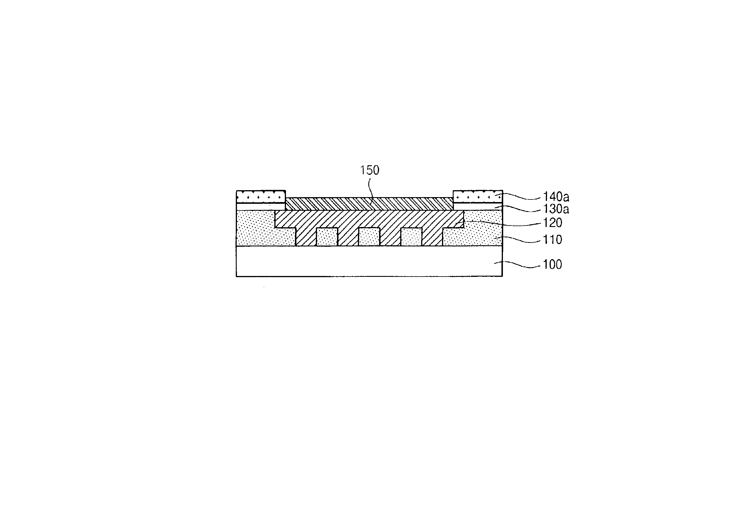
First, as shown in FIG. 2a, an insulation film pattern 100 including vias A and trenches B (i.e., a double Damascene pattern) is formed on a semiconductor substrate 100. In some cases, an additional copper wire may be formed between the semiconductor substrate 110 and the insulation film pattern 110. However, it is assumed that such an additional copper wire is not formed in the embodiment of the present invention.

More specifically, the insulation film pattern 110 is formed as follows...


PUM

PropertyMeasurementUnit
temperatureaaaaaaaaaa
thicknessaaaaaaaaaa

Abstract

Disclosed is a method of forming a copper wire on a semiconductor device capable of preventing the natural oxidation of copper. The method comprises the steps of: forming an insulation film pattern having vias and trenches on a semiconductor substrate; forming a copper wire by filling up the vias and the trenches with copper; successively forming a capping layer and a protective layer on the copper wire and the insulation film pattern; exposing the copper wire by selectively removing the capping layer and the protective layer; and forming an oxidation-prevention layer on the copper wire. According to the present invention, the natural oxidation of copper is avoided by selectively depositing aluminum on a copper wire pad, and therefore a dependable evaluation is possible from tests of reliability in a high temperature. Furthermore, since aluminum has a lower contact resistance compared with copper, dependable test results are obtained during tests of electrical characteristics.

Description

BACKGROUND OF THE INVENTION1. Field of the InventionThe present invention relates to a method of forming a copper wire on a semiconductor device, and more particularly to a method of forming a copper wire on a semiconductor device that prevents the natural oxidation of copper.2. Description of the Prior ArtLately, semiconductor devices are becoming more integrated and their processing technologies are correspondingly being improved. Therefore, a process using copper (Cu), instead of aluminum (Al) as in the prior art, for making a wire has been proposed as an effort to make speed, resistance or parasitic capacitance between metals of the devices. Moreover, instead of an insulation film made of an oxide as used in the prior art, an insulation film made of a material with a low dielectric constant has been highlighted in the process for making wires for semiconductor devices of the next generation.However, a wire-making process using copper and materials with low dielectric constants i...

Claims


Application Information

Patent Timeline
Patent Type & Authority Patents(United States)
IPC IPC(8): H01L21/285H01L21/70H01L21/02H01L21/768H01L21/28
CPCH01L21/28562H01L21/76879H01L21/76849H01L21/28
Inventor LEE, BYUNG ZUKIM, HYUN YONG
Owner CHUNG CHENG HLDG LLC
Why Eureka
Try Eureka