Photovoltaic device and manufacturing method thereof

a photovoltaic device and manufacturing method technology, applied in the direction of sustainable manufacturing/processing, instruments, final product manufacturing, etc., can solve the problems of adversely affecting the p-n junction characteristics or bsf effect, difficult to completely remove water or organic matter on the surface of the substrate, etc., to improve the open circuit voltage, improve the junction characteristics, and improve the interface characteristics

Inactive Publication Date: 2005-04-12
SANYO ELECTRIC CO LTD
View PDF3 Cites 40 Cited by
  • Summary
  • Abstract
  • Description
  • Claims
  • Application Information

AI Technical Summary

Benefits of technology

[0014]The present invention was made to solve the above-mentioned conventional problem and to improve interface characteristics between a crystalline semiconductor and an amorphous semiconductor thin film so that junction characteristics can be upgraded. In a semiconductor device according to the present invention, especially in a solar cell device, it is an object of the present invention to improve open circuit voltage.
[0019]As described above, in a p-n junction formed from a crystalline semiconductor and an amorphous semiconductor thin film, junction characteristics may be improved by interposing an appropriate amount of one conductive type or other conductive type impurity in the vicinity of an interface between a substrate of a crystalline semiconductor and an amorphous semiconductor thin film to suppress recombination of carriers at the interface. Open circuit voltage can be improved in a solar cell using this junction.
[0020]Also in a BSF structure comprising the crystalline semiconductor and a substantially intrinsic amorphous semiconductor thin film, electron flow may be improved by interposing an appropriate amount of one conductive type or another conductive type impurity in the vicinity of an interface between a substrate of a crystalline semiconductor and an amorphous semiconductor thin film to moderate an effect of band offset, which leads to improvement of open circuit voltage.

Problems solved by technology

Therefore, good interface characteristics can be achieved even with an impure substrate, which is subject to an adverse effect of impurity or deficiency of oxygen induction under a high temperature process.
Because of this low temperature process, it is difficult to remove water or organic matters on the surface of the substrate completely.
Degraded interface characteristics caused by these impurities may adversely affect the p-n junction characteristics or BSF effect.

Method used


Image

  • Photovoltaic device and manufacturing method thereof
  • Photovoltaic device and manufacturing method thereof
  • Photovoltaic device and manufacturing method thereof

Examples


fourth embodiment

ing a relation between an output (Pmax) of the photovoltaic device and the atomy density of phosphorous at an interface on a rear surface side.

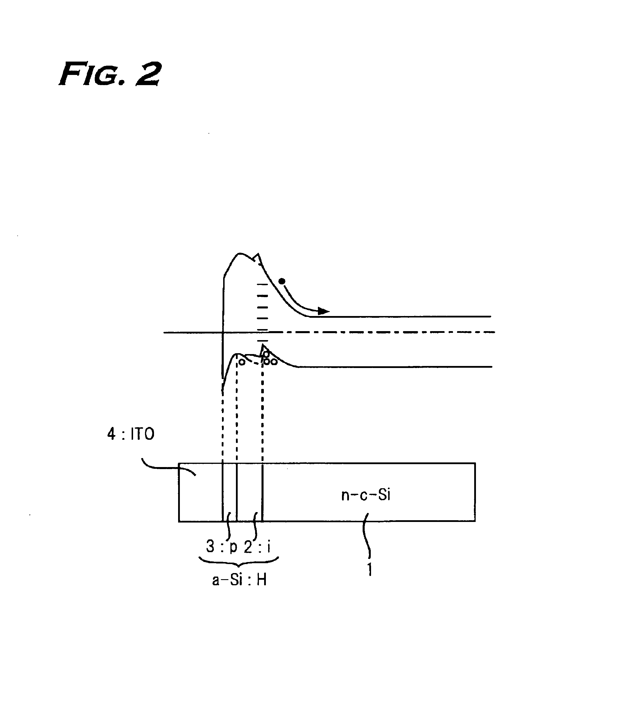
[0032]FIG. 8 is a perspective view illustrating a photovoltaic device wherein a surface of a single crystalline silicon substrate is textured and an i-type amorphous semiconductor layer is interposed on a junction interface between the crystalline semiconductor and an amorphous semiconductor.

[0033]The foregoing and other objects, features, aspects and advantages of the present invention will become more apparent from the following detailed description of the present invention when reviewed in conjunction with the accompanying drawings.

DESCRIPTION OF THE PREFERRED EMBODIMENTS

[0034]Now explanations are made of embodiments according to the present invention by referring to the drawings.

[0035](First embodiment)

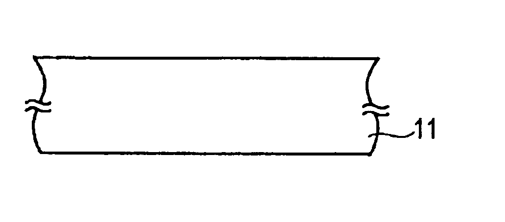
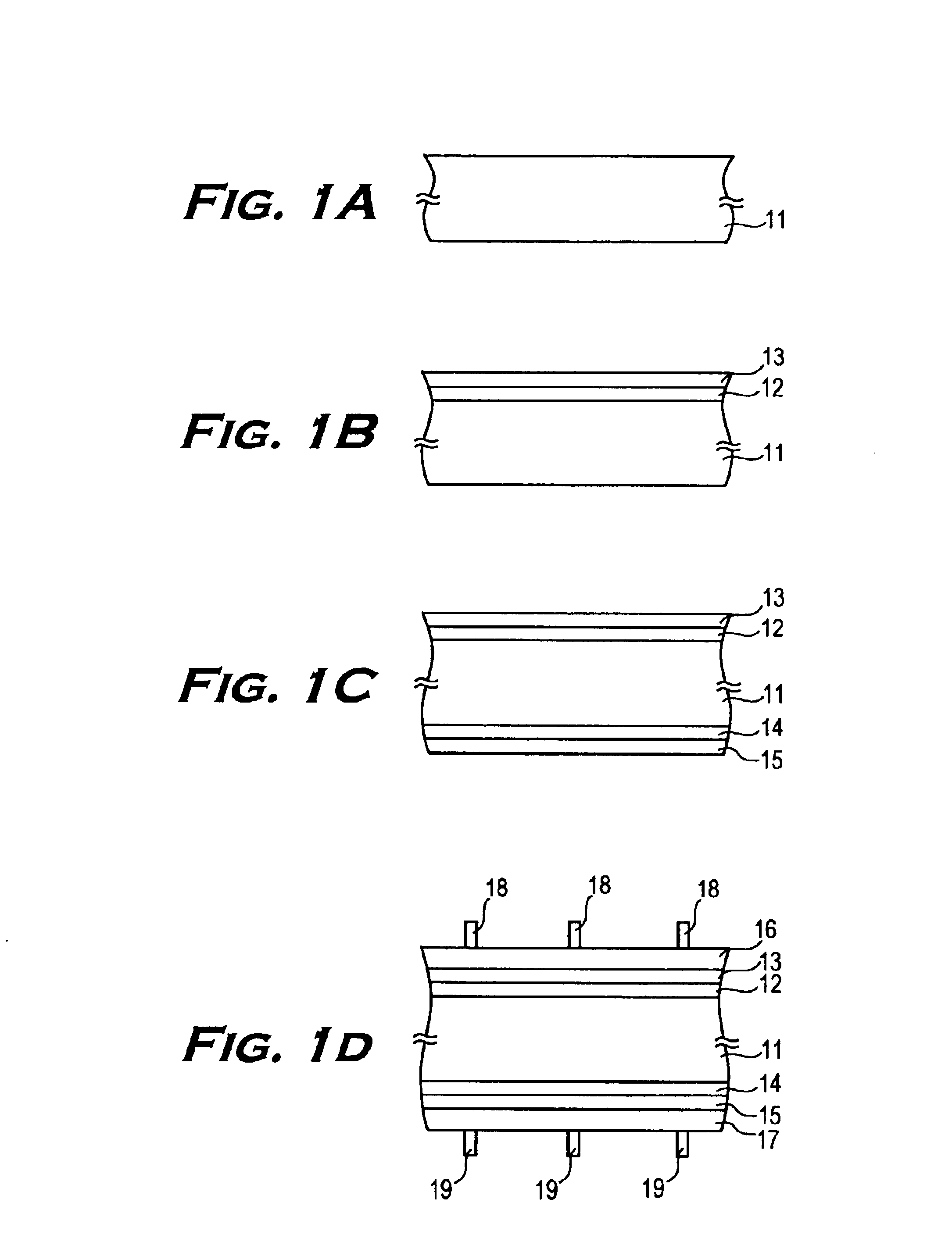
[0036]FIG. 1A to 1D are cross sectional views illustrating manufacturing processes of a photovoltaic device according to the first embodi...


PUM

PropertyMeasurementUnit
temperatureaaaaaaaaaa
thicknessaaaaaaaaaa
thicknessaaaaaaaaaa

Abstract

A photovoltaic device having a crystalline semiconductor and an amorphous semiconductor thin film so that junction characteristics can be upgraded. The photovoltaic device includes an i-type amorphous silicon thin film and a p-type amorphous silicon thin layer laminated in this order on a front surface of an n-type single crystalline silicon substrate, and an i-type amorphous silicon layer and an n-type amorphous silicon layer laminated in this order on a rear surface of the single crystalline silicon substrate, wherein an i-type amorphous silicon film is formed after the front surface of the single crystalline silicon substrate is exposed to a plasma discharge using mixed gas of hydrogen gas and a gas containing boron so that atoms of boron may be interposed on an interface between the single crystalline silicon substrate and the i-type amorphous silicon layer.

Description

BACKGROUND OF THE INVENTION[0002]1. Field of the Invention[0003]The present invention relates to a photovoltaic device utilizing a hetero semiconductor junction and a manufacturing method thereof.[0004]2. Description of Related Art[0005]A photovoltaic device is generally categorized into single crystalline-, polycrystalline-, and amorphous-based type depending on a type of a semiconductor of a part for converting absorbed light mainly into electric current. By the way, a hybrid type photovoltaic device taking both advantages of an amorphous semiconductor thin film and a crystalline semiconductor is studied (JP, H04-130671, A). In this photovoltaic device, an intrinsic amorphous silicon thin film without dopant of a conductive impurity or a substantially intrinsic amorphous silicon thin film doped with a small amount of an element in the 3A group of the periodic table such as boron is interposed on a junction interface in forming a semiconductor junction by combining a crystalline si...

Claims


Application Information

Patent Timeline
Patent Type & Authority Patents(United States)
IPC IPC(8): H01L31/18H01L31/06H01L31/075H01L31/20H01L31/04C23C16/24H01L31/0747
CPCH01L31/0747H01L31/075H01L31/202Y02E10/547Y02E10/548Y02P70/50
Inventor TAGUCHI, MIKIOASAUMI, TOSHIOTERAKAWA, AKIRA
Owner SANYO ELECTRIC CO LTD
Why Eureka
Try Eureka