
Flexible connecting device for interfacing with a wafer

Active Publication Date: 2005-04-12
XENOGENIC DEV LLC
View PDF6 Cites 7 Cited by
  • Summary
  • Abstract
  • Description
  • Claims
  • Application Information

AI Technical Summary

Benefits of technology

As embodied and broadly described herein, the present invention provides a connecting device for connecting to a body of semiconductor material that includes an integrated circuit. The body of semiconductor material further includes a planar surface with a plurality of clusters that have a plurality of signal transmissive connector elements arranged in a predetermined disposition. The connecting device carries a plurality of groups of signal transmissive connector members, wherein each group of signal transmissive connector members is associated with a respective cluster of signal transmissive connector elements. The signal transmissive connector members in each group are arranged according to the disposition of the signal transmissive connector elements in the cluster associated with that group, such that each signal transmissive connector member mates with a corresponding one of the signal transmissive connector elements. The connecting device further includes flexible portions between its respective groups of signal transmissive connector members, and each flexible portion includes a plurality of signal transmission pathways connecting to a respective signal transmissive connector member of a group of signal transmissive connector members. The flexible portions have a flexibility that allows the respective groups of signal transmissive connector members to move in relation to one another under the effect of thermal expansion of the body of semiconductor material.
The connecting device described above provides the advantage of having flexible portions located between its groups of signal transmissive connector members. These flexible portions allow the groups of signal transmissive connector members to move in relation to each other when they are connected to respective clusters of signal transmissive connector elements on the surface of a body of semiconductor material. As such, each group of signal transmissive connector members is able to maintain a secure and undamaged connection with a respective cluster of signal transmissive connector elements as the body of semiconductor material expands and contracts under thermal effects.
The connecting device further includes flexible portions between each group of signal transmissive connector members that allow the groups of signal transmissive connector members to move in relation to each other. In a non-limiting example of implementation, the flexible portions can be in the form of a flexible printed circuit. The flexible printed circuit includes a flexible insulating membrane on which are formed by printing, one or more bundles of signal transmission pathways. The flexible portions have sufficient flexibility to allow the groups of signal transmissive connector members to move a distance that is in accordance with the thermal expansion and contraction of the body of semiconductor material.
As further embodied and broadly described herein, the present invention provides a connecting device for a body of semiconductor material that includes an integrated circuit. The body of semiconductor material has a planar surface with a plurality of optical signal transmissive connector elements arranged in a predetermined disposition thereon. The connecting device comprises a plurality of optical signal transmissive connector members that are each associated with a respective optical signal transmissive connector element. The optical signal transmissive connector members are arranged according to the disposition of the optical signal transmissive connector elements such that each optical signal transmissive connector member can communicate optically with a corresponding one of the optical signal transmissive connector elements. The connecting device further includes flexible portions between respective optical signal transmissive connector members. Each flexible portion includes a signal transmission pathway that connects to an optical signal transmissive connector member. The flexible portions have a flexibility that allows respective optical signal transmissive connector members to move in a direction parallel to the planar surface in relation to one another under the effect of thermal expansion of the body of semiconductor material.

Problems solved by technology

Presently, integrated circuits are becoming increasingly large.
A problem with such large integrated circuits is that they comprise more than one cluster of signal transmissive connector elements, and the separation between the clusters changes as the body of semiconductor material expands and contracts under thermal effects.
Unfortunately, traditional connecting devices do not have the same coefficient of thermal expansion as the body of semiconductor material.
Therefore, as the body of semiconductor material heats up, the expansion of the distance between the clusters of signal transmissive connector elements causes strain on the connections between the clusters of signal transmissive connector elements and the connecting device.
Often, this strain is enough to damage and break the connection.

Method used


Image

  • Flexible connecting device for interfacing with a wafer
  • Flexible connecting device for interfacing with a wafer
  • Flexible connecting device for interfacing with a wafer

Examples


first embodiment

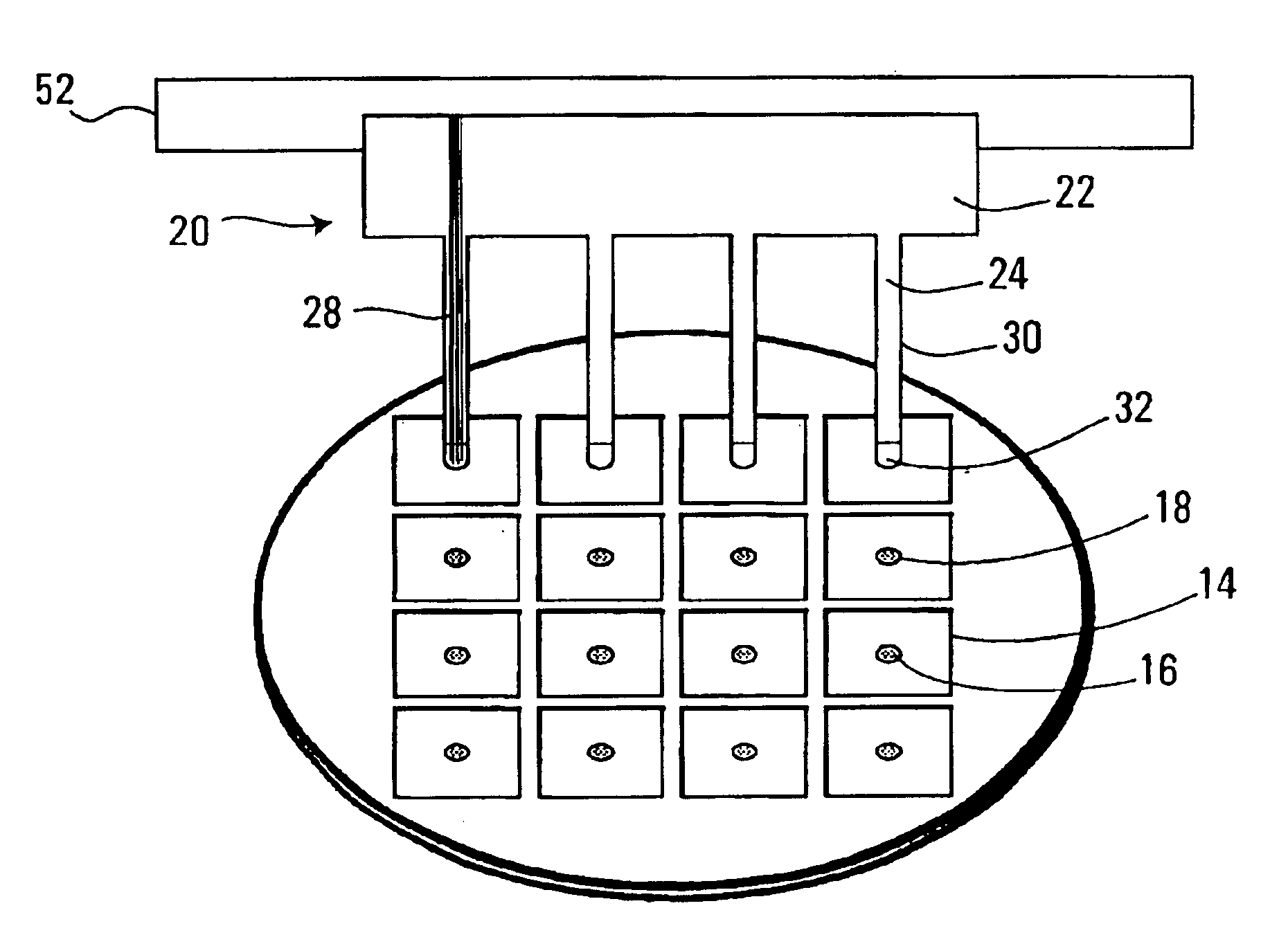
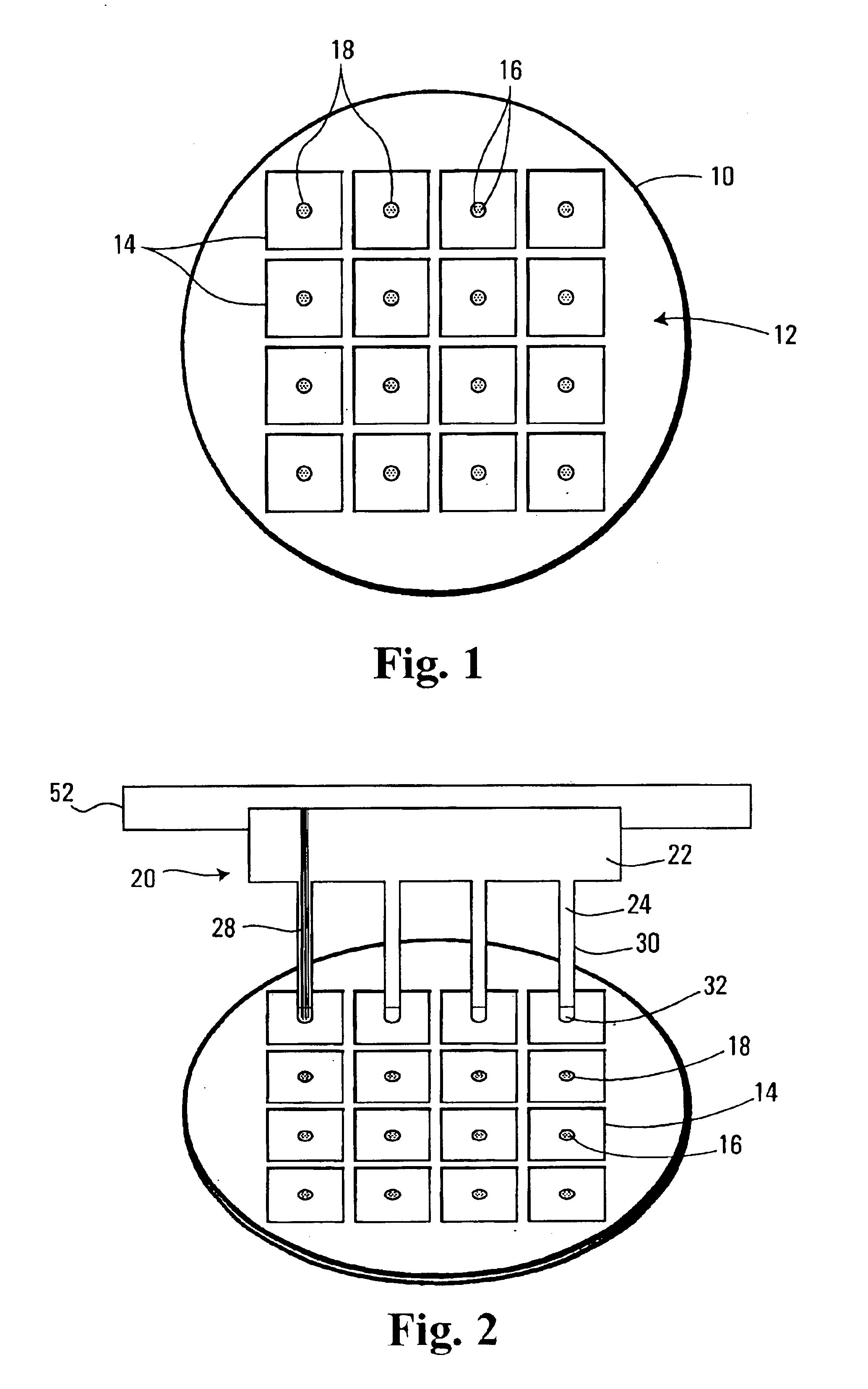
FIG. 2 shows a connecting device 20 in accordance with the present invention connected to semiconductor wafer 10. Connecting device 20 is adapted to connect the signal transmissive connector elements 16 located on wafer 10 to external devices such as terminal block 52, that in turn connects integrated circuit 12 to external circuitry (not shown). Connecting device 20 includes a base element 22 and a series of fingers 24. Each finger 24 comprises a finger body 30 and a fingertip 32. In the embodiment shown in FIG. 2, connecting device 20 includes a row of fingers 24 connected to a row of clusters 18, where each cluster 18 belongs to a respective functional module 14 in a row of functional modules.

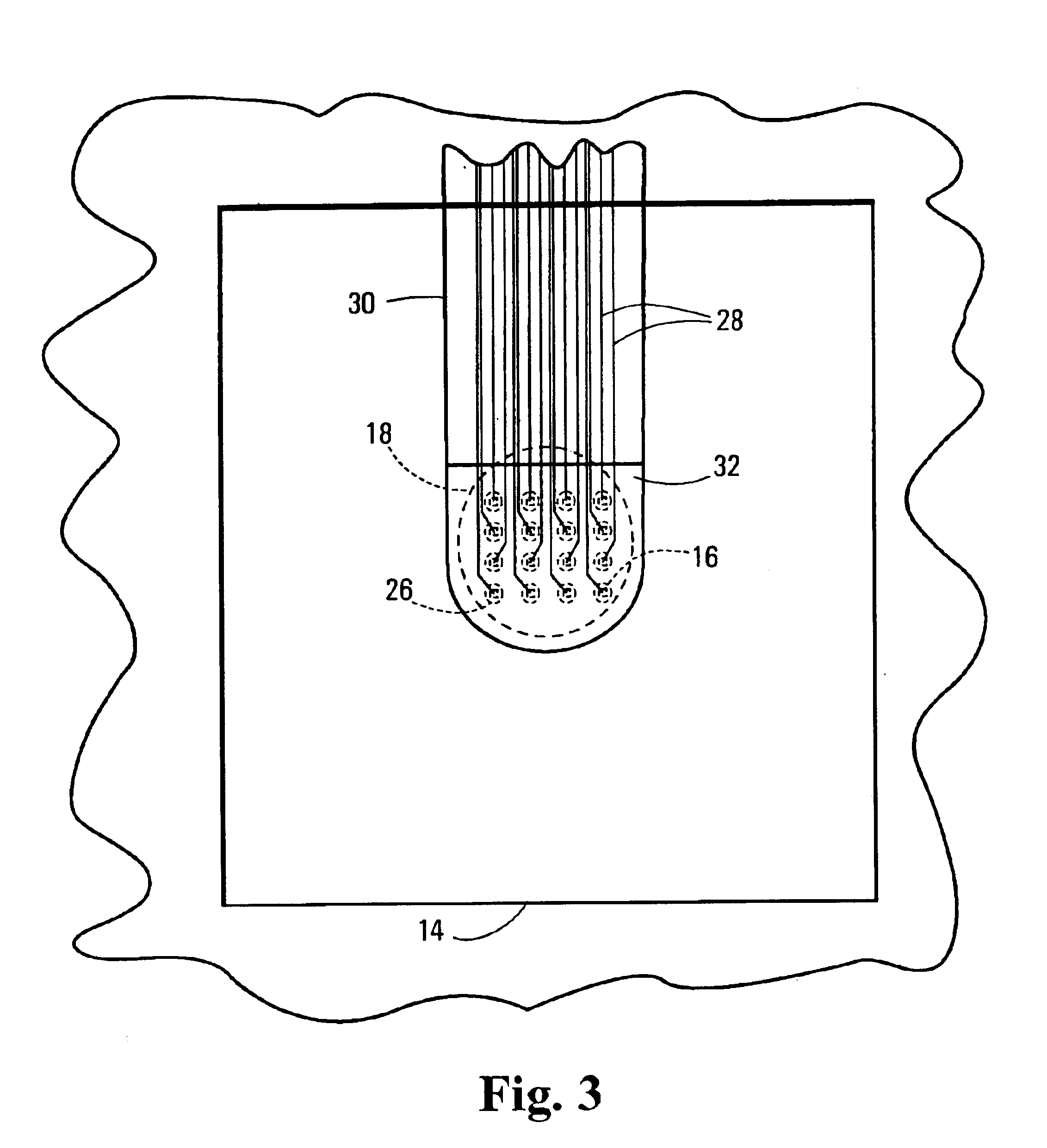
FIG. 3 is an expanded view of, fingertip 32 connected to a cluster 18 located within functional module 14. Although only one fingertip 32 is shown in FIG. 3, each fingertip 32 includes a group of signal transmissive connector members 26 for connection to signal transmissive connector element...

second embodiment

FIG. 6 is a top perspective view of a connecting device 42 in accordance with the present invention. Connecting device 42 includes a base element 44, and a long flexible band 34. Situated on band 34 are connector zones 38 and bowed flexible portions 36 that join connector zones 38.

Each connector zone 38 includes a group of signal transmissive connector members (not shown) for connecting to a corresponding cluster 18 of signal transmissive connector elements 16 on the surface of wafer 10. As discussed earlier in connection with the first embodiment the signal transmissive connector members within each group are arranged in a predetermined disposition that matches the disposition of the signal transmissive connector elements 16 in corresponding clusters 18. In this manner, when the connector zones 38 are placed over corresponding functional modules in a row of functional modules, the signal transmissive connector members in each group mate with their respective signal transmissive con...

third embodiment

FIG. 10 illustrates a connecting device 56 in accordance with the present invention, positioned above a wafer 52. Wafer 52 includes a planar surface with a plurality of functional modules 51 positioned thereon. Each functional module 51 includes an optical signal transmissive connector element 54 that is capable of transmitting and receiving optical signals. In the specific embodiment shown, optical signal transmissive connector elements 54 are shaped as conical recesses that extend into the surface of wafer 52. Each functional module 51 includes circuitry such as a wavelength filter and a wavelength converter, and an optical / electric converter for converting optical signals to electrical signals and vice versa. Circuitry for converting optical signals to electrical signals is known in the art, and will not be discussed in more detail herein. It should be understood that as wafer 52 expands and contracts under thermal effects, the distance between each optical signal transmissive co...


PUM


Abstract

The present invention provides a connecting device for connection to a body of semiconductor material. The body of semiconductor material includes an integrated circuit that contains a plurality of clusters of signal transmissive connector elements arranged in a predetermined disposition. The connecting device includes a plurality of groups of signal transmissive connector members for connection to an associated cluster of signal transmissive connector elements. The disposition of the signal transmissive connector members in each group matches the disposition of the signal transmissive connector elements in that group's associated cluster. The connecting device further includes flexible portions between its respective groups of signal transmissive connector members. The flexible portions have a flexibility that allows the groups of signal transmissive connector members to move in relation to each other when they are connected to respective clusters of signal transmissive connector elements on the surface of a body of semiconductor material. As such, each group of signal transmissive connector members is able to maintain a secure and undamaged connection with a respective cluster of signal transmissive connector elements as the body of semiconductor material expands and contracts under thermal effects.

Description

FIELD OF THE INVENTIONThe present invention provides a flexible connecting device for connecting to an integrated circuit located on a body of semiconductor material. More specifically the present invention provides a flexible connecting device that is able to adapt to the thermal expansion and contraction of a body of semiconductor material.BACKGROUND OF THE INVENTIONIn the past and to a certain extent still today, many integrated circuits are formed by etching a plurality of individual functional modules, or a group of a few interconnected functional modules onto the surface of a body of semiconductor material. Once the functional modules are formed onto the body of semiconductor material, each individual functional module, or the group of a few functional modules are cut out of the semiconductor material and are packaged as individual integrated circuits. Each integrated circuit comprises a cluster of signal transmissive connector elements that can be connected to external circui...

Claims


Application Information

Patent Timeline
IPC IPC(8): H01L23/52H01L23/538H01R12/62
CPCH01L23/5387H01L24/50H01R12/62H01L2924/14H01L24/86H01L2924/00
Inventor NORMAN, RICHARDCHAMBERLAIN, DAVID
Owner XENOGENIC DEV LLC
Features
  • Generate Ideas
  • Intellectual Property
  • Life Sciences
  • Materials
  • Tech Scout
  • Unparalleled Data Quality
  • Higher Quality Content
  • 60% Fewer Hallucinations
Learn More