High-performance programmable logic architecture

a logic architecture and high-performance technology, applied in the field of programmable logic integrated circuits, can solve the problems of general purpose programmable logic devices not being specially designed for special applications, devices also meeting with certain limitations, and general purpose devices having significant drawbacks, etc., to achieve the effect of arranging design

Inactive Publication Date: 2005-04-19
ALTERA CORP +1
View PDF58 Cites 14 Cited by
  • Summary
  • Abstract
  • Description
  • Claims
  • Application Information

AI Technical Summary

Benefits of technology

[0012]The present invention is a programmable logic device architecture. The architecture provides flexibility and a great deal of design routability. Many features of the architecture of the present invention are especially well-suited for use in emulation and rapid prototyping applications.
[0015]In the present invention, the internal circuitry of the various logic blocks may be monitored through a variety of programmable interconnect paths. This architecture is useful when debugging a design, especially for emulation and prototyping applications. For example, the present architecture provides, among other features: predictable logic, routing, and pin-out capacity; predictable and easily modified timing characteristics; and user-available diagnostic capabilities, including state observability. The present architecture may be used for debugging intensive applications where the probability of placement and routing success per chip is more of a concern than the operating speed path of the completed system.

Problems solved by technology

While such devices have met with substantial success, such devices also meet with certain limitations, especially in situations in which the provision of more complex logic modules and additional or alternative types of interconnections between the logic modules would have benefits sufficient to justify the additional circuitry and programming complexity.
Furthermore, general purpose programmable logic devices are not generally especially designed for special applications such as emulation and ASIC prototyping.
While these general purpose programmable logic devices may have served adequately in the initial development of these applications, it has become increasingly clear that for these applications, general purpose devices have some significant drawbacks.
However, with a general purpose programmable logic architecture, there is always a possibility that a given design or partition may not be implementable even through the gate count is within the rated capacity of the chip.
General purpose programmable logic devices have also typically not supported easy user-probing of internal state information inside the integrated circuit.
If any (one or more) particular design partition does not fit into the assigned programmable logic chip, then the whole system will not be properly implemented.
Furthermore, when partitioning large designs into a number of programmable logic chips, it is desirable that the timing of the original netlist be preserved, which may not be the case if the programmable logic architecture does not provide features to allow this.
When partitioning designs into a number of chips, signal path delays may be expanded, but not necessarily uniformly.
These differences in signal path delays may introduce timing problems including skews, setup, and hold time violations which are not inherent in the design netlist.
Furthermore, timing problems which are present in the design netlist will be hidden by the mapping into multiple programmable logic devices.
Existing programmable logic architectures generally do not include adequate means for detecting these types of introduced timing problems and effective means for removing these problems.

Method used


Image

  • High-performance programmable logic architecture
  • High-performance programmable logic architecture
  • High-performance programmable logic architecture

Examples


Embodiment Construction

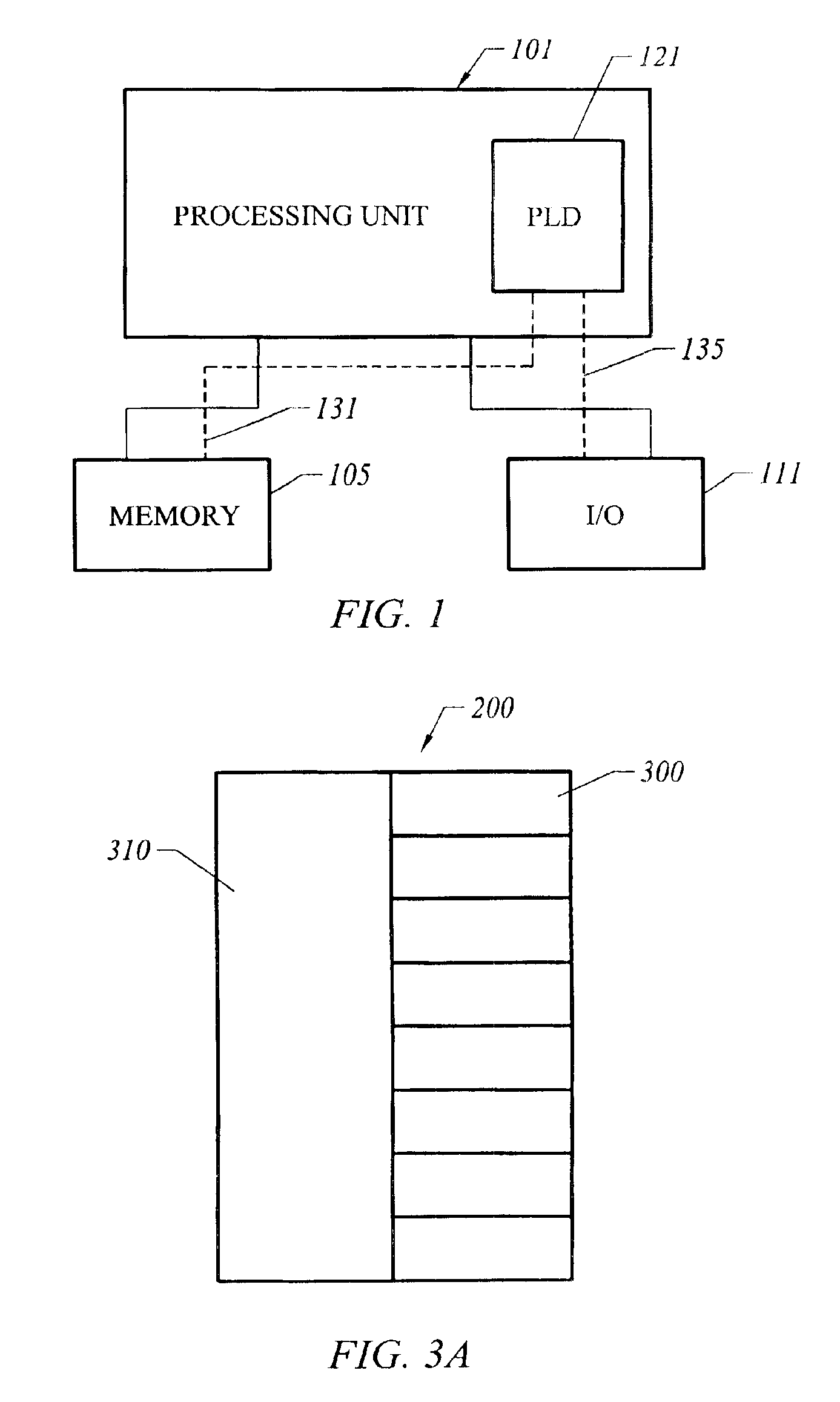
[0030]FIG. 1 shows a block diagram of a digital system within which the present invention may be embodied. The system may be provided on a single board, on multiple boards, or even within multiple enclosures. FIG. 1 illustrates a system 101 in which a programmable logic device 121 may be utilized. Programmable logic devices (sometimes referred to as a PALS, PLAs, FPLAs, PLDs, EPLDs, EEPLDs, LCAs, or FPGAs), are well known integrated circuits that provide the advantages of fixed integrated circuits with the flexibility of custom integrated circuits. Such devices allow a user to electrically program standard, off the shelf logic elements to meet a user's specific needs. See, for example, U.S. Pat. No. 4,617,479, incorporated herein by reference for all purposes. Such devices are currently represented by, for example, Altera's MAX® series of PLDs and FLEX® series of PLDs. The former are described in, for example, U.S. Pat. Nos. 5,241,224 and 4,871,930, and the Altera Data Book, March 1...


PUM


Abstract

A programmable logic device architecture. This programmable logic architecture includes a first logic block (425) containing programmable logic elements for performing logic functions. The architecture may also include a diagnostic block interface (415), which interfaces with the first logic block (425), for performing JTAG functions, configuring the first logic block (425), initializing the first logic block (425), interfacing with off-chip diagnostic and test devices and equipment, and performing other similar functions. The first logic block (425) may be programmably coupled to other components on the integrated circuit using a first programmable interconnect network (511). The first logic block (425) includes a plurality of second logic blocks (505) which may be programmably coupled using a second programmable interconnect network (521). The second programmable interconnect network (521) may be programmably coupled to the first programmable interconnect network (511). Furthermore, the plurality of second logic blocks (505) include a plurality of third logic blocks (525) which may be programmably coupled using a third programmable interconnect network (535). A signal from a third logic block (525) may be programmably coupled to the other logic blocks, the diagnostic block interface (415), and other circuitry on the integrated circuit. The internal circuitry of these logic blocks may be monitored through a variety of programmable interconnect paths. This architecture is useful when debugging a design, especially for emulation and prototyping applications.

Description

CROSS-REFERENCES TO RELATED APPLICATIONS[0001]This application is a continuation of U.S. patent application Ser. No. 08 / 824,535, filed Mar. 26, 1997 now U.S. Pat. No. 6,570,404, which claims the benefit of U.S. Provisional Application No. 60 / 014,440, filed Mar. 29, 1996, which are incorporated by reference.BACKGROUND OF THE INVENTION[0002]The present invention relates to the field of programmable logic integrated circuits. More specifically, the present invention provides an enhanced programmable logic architecture, improving upon the composition, configuration, and arrangements of logic array blocks (LABs) and logic elements (LEs) and also the interconnections between these logic array blocks and logic elements.[0003]Programmable Logic Devices (PLDs) are well known to those in the electronic art. Such programmable logic devices are commonly referred as PALs (Programmable Array Logic), PLAs (Programmable Logic Arrays), FPLAs (Field Programmable Logic Arrays), PLDs (Programmable Logi...

Claims


Application Information

Patent Timeline
Patent Type & Authority Patents(United States)
IPC IPC(8): H03K19/177
CPCH03K19/17704H03K19/17764H03K19/17736H03K19/17728
Inventor NORMAN, KEVIN A.PATEL, RAKESH H.SAMPLE, STEPHEN P.BUTTS, MICHAEL R.
Owner ALTERA CORP
Why Eureka
Try Eureka