Tristate structures for programmable logic devices

a technology of programmable logic and device, applied in the direction of computation using denominational number representation, pulse technique, instruments, etc., can solve the problems of devices also meeting with certain limitations, and achieve the effects of greater utilization and flexibility, and improved performance and operating characteristics

Inactive Publication Date: 2005-04-19
ALTERA CORP
View PDF37 Cites 39 Cited by
  • Summary
  • Abstract
  • Description
  • Claims
  • Application Information

AI Technical Summary

Benefits of technology

[0011]The tristate driver of the present invention may buffer and drive an input signal to an output line. This tristate driver may provide sufficient drive capability for driving a programmable interconnect conductor, which may be relatively heavily loaded. The tristate driver may be programmably and logically controlled. More specifically, the tristate driver may be programmably disabled, where its output will be tristated regardless of the states of logical inputs. When programmably enabled, the tristate driver output will be tristated or enabled depending on the states of the logical inputs. When logically and programmably enabled, the input line will be driven to the output line.
[0012]The architecture of the present invention provides greater utilization and flexibility in using the programmable and global interconnect structures of the programmable logic device. The architecture also provides greater utilization and flexibility in using the logic elements and other programmable resources. Furthermore, the programmable logic functions in this architecture may be dynamically and logically reconfigured, without the need to reprogram programmable cells. Further, the architecture of the present invention provides better performance and operating characteristics, including improved transient response.

Problems solved by technology

While such devices have met with substantial success, such devices also meet with certain limitations, especially in situations in which the provision of more complex logic modules and additional or alternative types of interconnections between the logic modules would have benefits sufficient to justify the additional circuitry and programming complexity.

Method used


Image

  • Tristate structures for programmable logic devices
  • Tristate structures for programmable logic devices
  • Tristate structures for programmable logic devices

Examples


Embodiment Construction

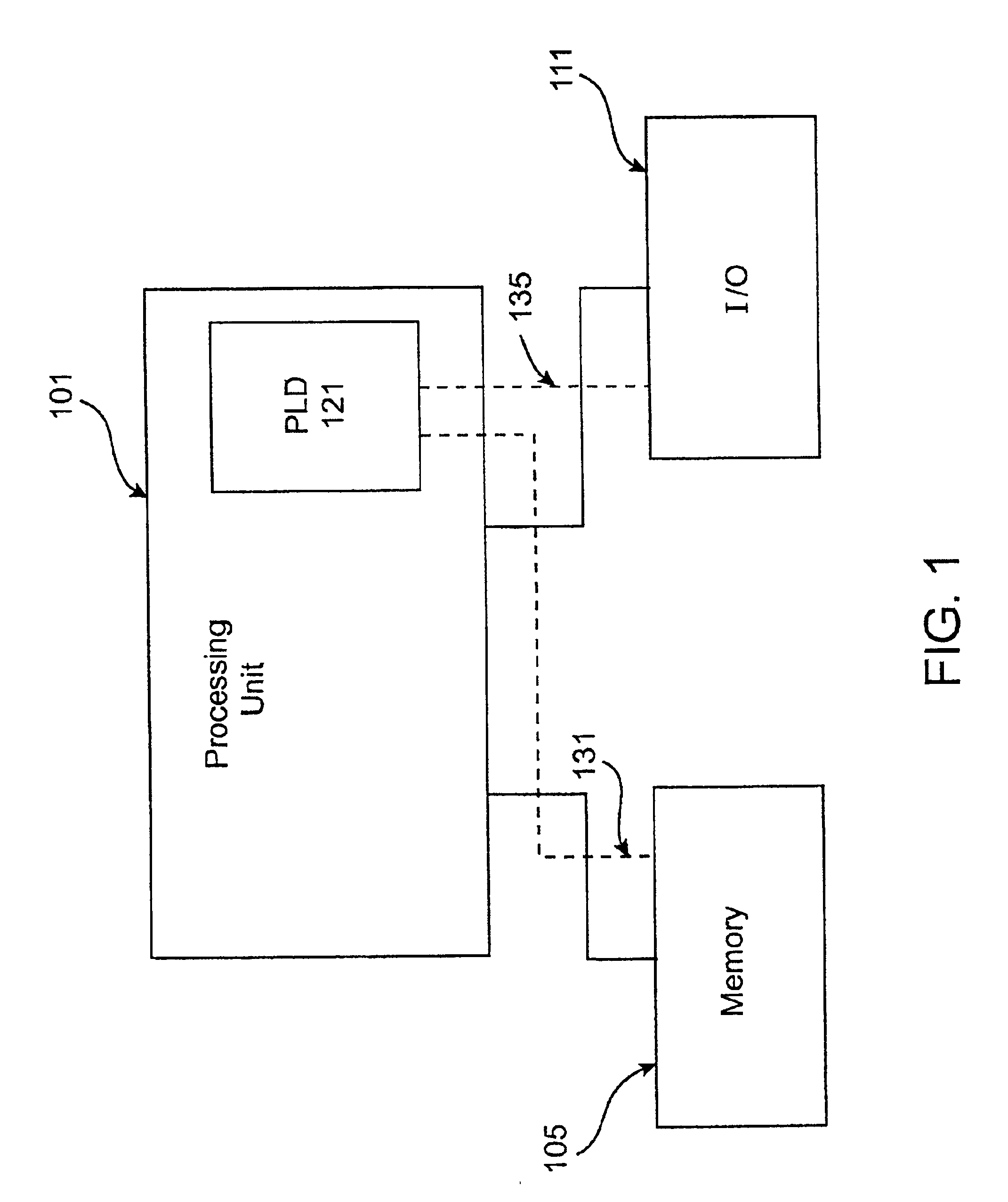
[0021]FIG. 1 shows a block diagram of a digital system within which the present invention may be embodied. In the particular embodiment of FIG. 1, a processing unit 101 is coupled to a memory 105 and an I / O 111 and incorporates a programmable logic device (PLD) 121. PLD 121 may be specially coupled to memory 105 through connection 131 and to I / O 111 through connection 135. The system may be a programmed digital computer system, digital signal processing system, specialized digital switching network, or other processing system. Moreover, the system may be a general purpose computer, a special purpose computer (such as telecommunications equipment) optimized for an application-specific task such as programming PLD 121, or a combination of a general purpose computer and auxiliary special purpose hardware.

[0022]Processing unit 101 may direct data to an appropriate system component for processing or storage, execute a program stored in memory 105 or input using I / O 111, or other similar ...


PUM


Abstract

A programmable logic device architecture including tristate structures. The programmable logic device architecture provides tristate structures which may be logically or programmably controlled, or both. Through these tristate structures, the logic elements may be coupled to the programmable interconnect, where they may be coupled with other logic elements of the programmable logic device. Using these tristate structures, the signal pathways of the architecture may be dynamically reconfigured.

Description

CROSS-REFERENCES TO RELATED APPLICATIONS[0001]This is a continuation application of U.S. patent application Ser. No. 09 / 169,207, filed Oct. 9, 1998, now U.S. Pat. No. 6,239,613, which is a divisional application of U.S. patent application Ser. No. 08 / 587,875, filed Jan. 10, 1996, issued as U.S. Pat. No. 5,894,228 on Apr. 13, 1999, all of which are incorporated by reference.BACKGROUND OF THE INVENTION[0002]The present invention relates to the field of programmable logic integrated circuits. More specifically, the present invention provides an enhanced programmable logic architecture, improving upon the composition, configuration, and arrangements of logic array blocks (LABs) and logic elements (LEs) and also the interconnections between these logic array blocks and logic elements.[0003]Programmable Logic Devices (PLDs) are well known to those in the electronic art. Such programmable logic devices are commonly referred as PALs (Programmable Array Logic), PLAs (Programmable Logic Array...

Claims


Application Information

Patent Timeline
Patent Type & Authority Patents(United States)
IPC IPC(8): H03K19/177
CPCH03K19/17728H03K19/17752H03K19/17736
Inventor REDDY, SRINIVASCLIFF, RICHARD G.
Owner ALTERA CORP
Why Eureka
Try Eureka