Method of manufacturing semiconductor device

a manufacturing method and semiconductor technology, applied in the direction of semiconductor devices, electrical devices, transistors, etc., can solve the problems of lowering the driving capability, reducing parasitic resistance, and raising the sheet resistance of the extension portions, so as to reduce parasitic resistance, improve the roll-off characteristic, and achieve sufficient driving capability

Inactive Publication Date: 2005-08-18
SONY CORP
View PDF2 Cites 12 Cited by
  • Summary
  • Abstract
  • Description
  • Claims
  • Application Information

AI Technical Summary

Benefits of technology

[0019] The present invention has been made based on the above-mentioned problems. Accordingly, it is an object of the present invention to provide a method of manufacturing a semiconductor device in which a halo implantation suited particularly to a fully depleted SOI-MOSFET provided with a thin film SOI layer is carried out to make it possible to simultaneously achieve an improvement of roll-off characteristic and a reduction in parasitic resistance and to secure a sufficient driving capability.
[0021] According to the present invention, the impurity for the reverse-characteristic layer can be introduced, in a sufficient concentration, into the body portion side of the extension portions. Namely, since the impurity for the reverse-characteristic layer is scarcely introduced into the extension portions, it is possible to simultaneously achieve suppression of a rise in parasitic resistance (suppression of a rise in sheet resistance in the extension portions) and an improvement of roll-off characteristic, and to secure a sufficient driving capability.
[0023] In addition, the present invention promises a conspicuous effect of improving the driving capability, in a semiconductor device in which the Si active layer region is so formed that a depleted layer induced at the body portion reaches the interface between the SOI layer and the buried oxide film in the SOI substrate.
[0028] According to the present invention, implantation energy and implantation angle are so adjusted that the range of projection in halo implantation reaches the buried oxide film of the SOI substrate, thereby forming the reverse-characteristic layer. By this, even in the case of a fully depleted SOI-MOSFET in which, for example, the SOI layer in the form of a thin film (for example, a thin film such that the depleted layer induced at the body portion reaches the interface between the SOI layer and the buried oxide film in the SOI substrate) is formed, it is possible to simultaneously achieve an improvement of roll-off characteristic and a reduction in parasitic resistance, and thereby to obtain an LSI with high speed and low power consumption which securely displays a sufficient driving capability.

Problems solved by technology

As a result, the sheet resistance in the source / drain portions and the extension portions is raised, i.e., the parasitic resistance of the transistor is raised, thereby lowering the driving capability.
However, in the case where the reverse-characteristic layer is formed on the lower surface side (the buried oxide film side) of the extension portions as shown in FIG. 10, particularly in a fully depleted SOI-MOSFET in which p-MOS is formed, there is the problem that the sheet resistance of the extension portions is raised.
Due to the foregoing, in the fully depleted SOI-MOSFET in which a thin film SOI layer is formed, it is impossible to simultaneously achieve an improvement of roll-off characteristic and a reduction in parasitic resistance, and, therefore, it has been impossible to secure a sufficient driving capability.

Method used


Image

  • Method of manufacturing semiconductor device
  • Method of manufacturing semiconductor device
  • Method of manufacturing semiconductor device

Examples


example

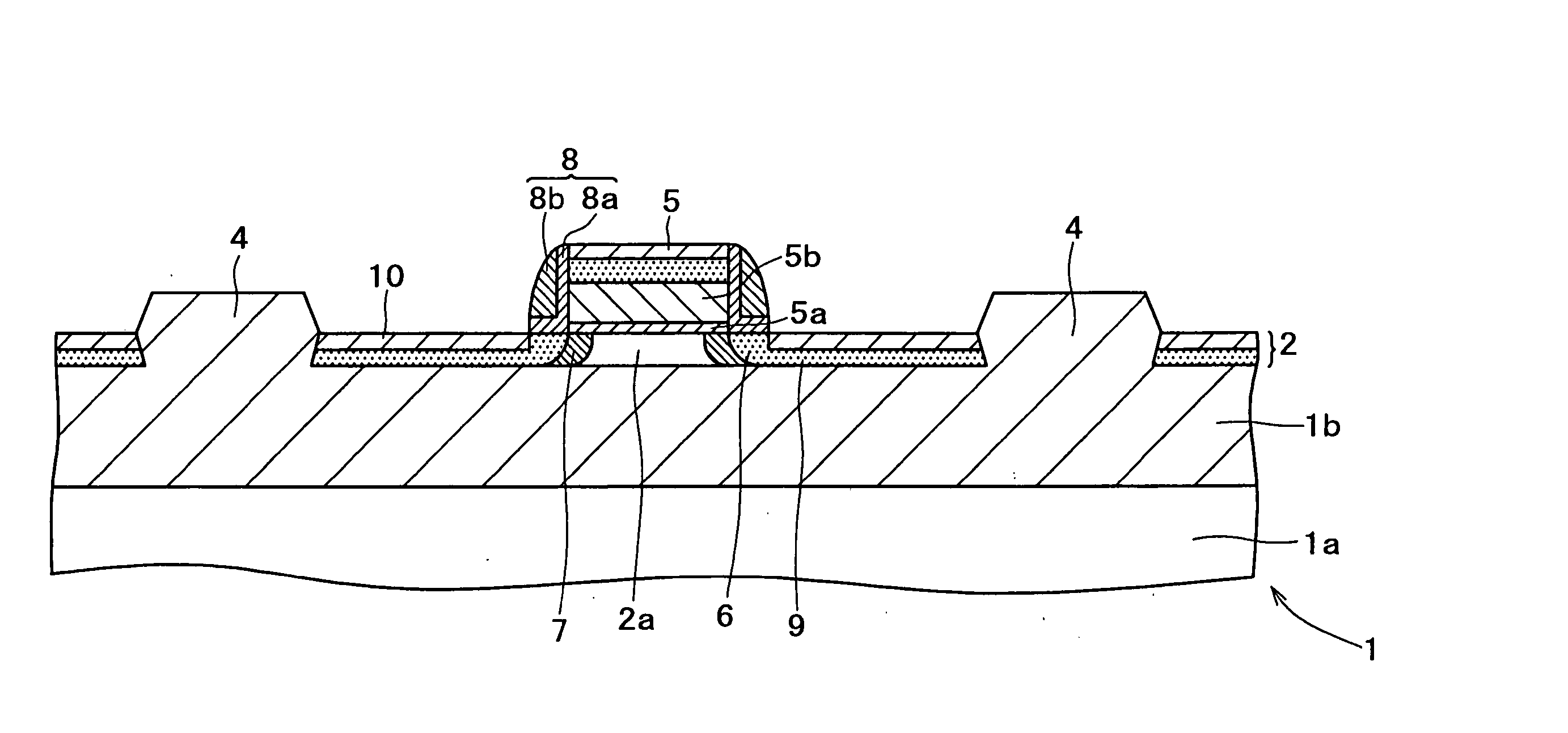
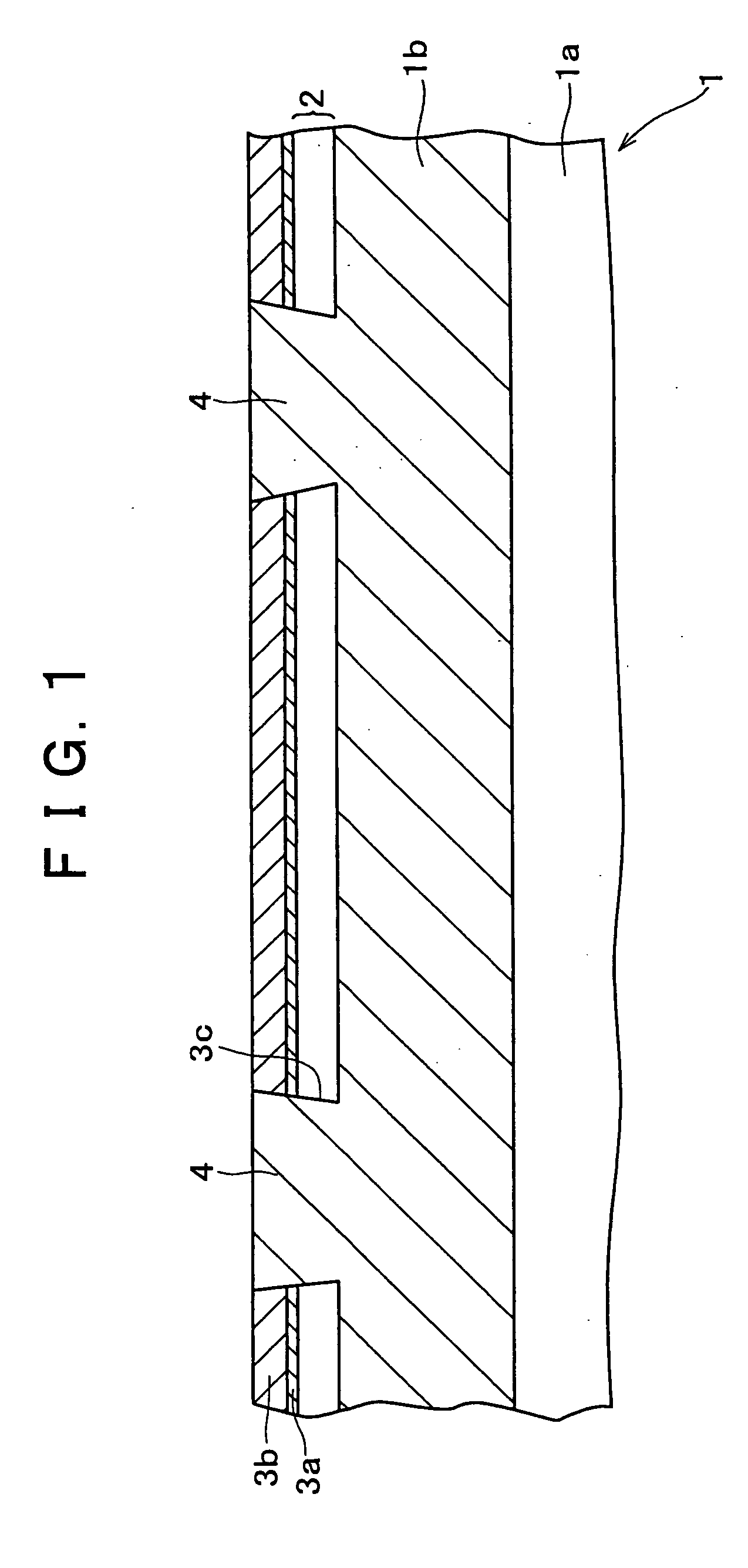
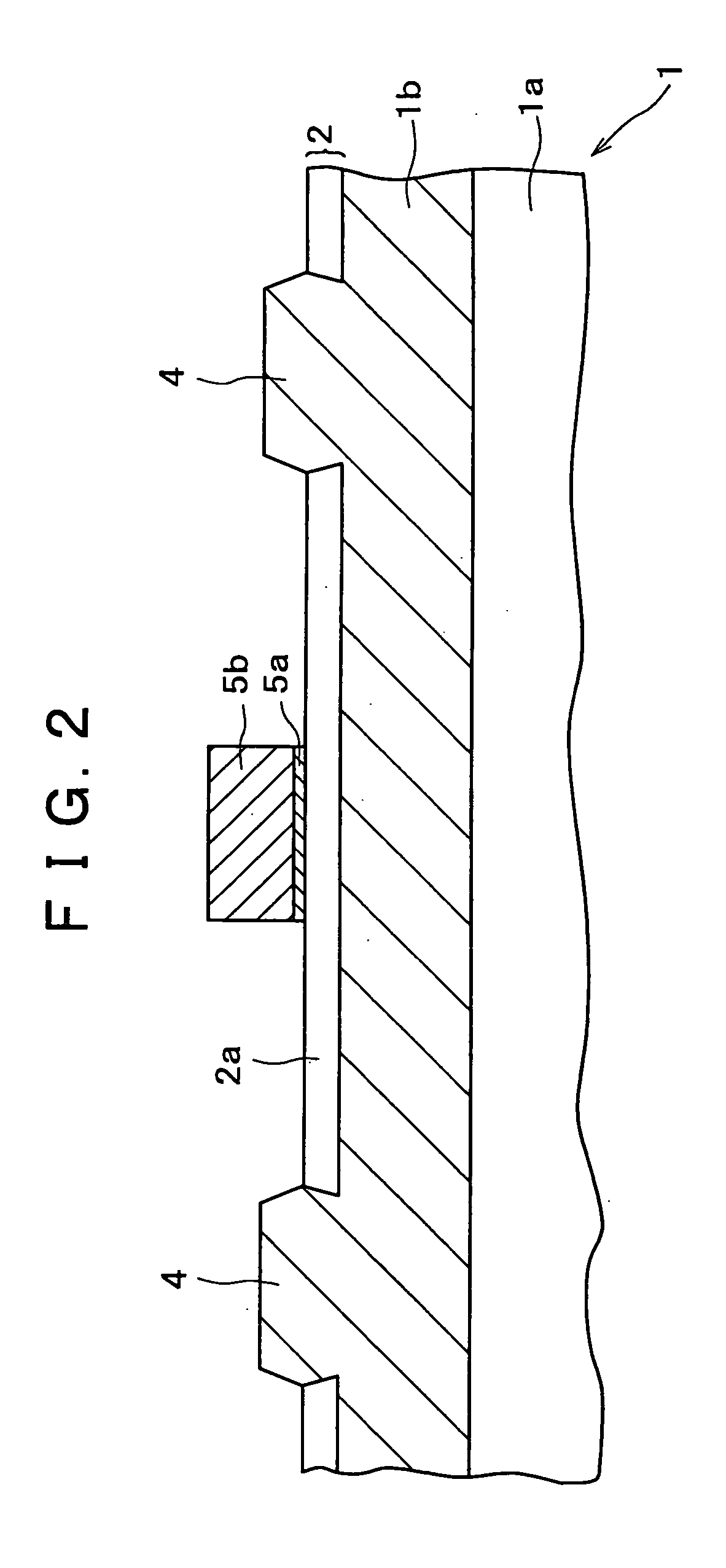
[0046] An example of the method of manufacturing a semiconductor device (SOI-MOSFET) according to the present embodiment will be described in detail below, based on the drawings (which show respective manufacturing steps). First, in FIG. 1, an SOI substrate 1 in which an SOI layer 2 in the form of a thin film (for example, 33 nm in thickness) is formed on an Si substrate 1a with a comparatively thick buried oxide film (for example, an oxide film of 100 nm in thickness) 1b therebetween was used, a thermal oxide film 3a (for example, 10 nm in thickness) was formed on the surface of the SOI layer 2 (upon this formation, the thickness of the SOI layer becomes about 29 nm), and thereafter an Si3N4 film 3b (for example, 100 nm in thickness) as a protective film for CMP (chemical mechanical polish) was formed on the surface of the thermal oxide film 3a by a low pressure CVD (low pressure chemical vapor deposition) method.

[0047] Then, only the portions of the Si3N4 film 3b where the device...


PUM


Abstract

Disclosed is a method of manufacturing a semiconductor device. A plurality of device separation regions are formed in an SOI layer of an SOI substrate, a desired impurity is implanted into a body portion of an Si active layer region, and therereafter a gate electrode is formed with a gate insulation film therebetween. Thereafter, an impurity is implanted into the Si active layer region to form extension portions of source / drain portions, and then an impurity different in polarity from the impurity in the source / drain portions is halo-implanted to form a reverse-characteristic layer. In the halo implantation, the range of projection is set to reach the inside of a buried oxide film. With this configuration, in a fully depleted SOI-MOSFET or the like provided with a thin film S0I layer, it is made possible to simultaneously achieve an improvement of roll-off characteristic and a reduction in parasitic resistance and to secure a sufficient driving capability.

Description

BACKGROUND OF THE INVENTION [0001] The present invention relates to a method of manufacturing a semiconductor device, and is for contriving a higher degree of integration and a higher performance in an LSI of, for example, a MOS transistor or the like which uses an SOI substrate. [0002] In recent years, in the LSI of the MOS transistor (hereinafter referred to as MOSFET), a higher degree of integration and a higher performance have been demanded, and a structure in which an SOI (silicon on insulator) layer is formed on a semiconductor substrate with a buried oxide layer therebetween, i.e., a MOSFET using an SOI substrate (hereinafter referred to as SOI-MOSFET) has been paid attention to. In the SOI-MOSFET, perfect device separation is achieved by an insulation layer (silicon oxide layer), so that soft errors and latch-up are suppressed, and high reliability can be obtained even in an LSI with a high degree of integration. In addition, since it is possible to reduce junction capacity...

Claims


Application Information

Patent Timeline
Patent Type & Authority Applications(United States)
IPC IPC(8): H01L21/336H01L21/762H01L29/45H01L29/786H01L21/265
CPCH01L21/76264H01L21/76283H01L29/78696H01L29/66772H01L29/458
Inventor KOYAMA, KAZUHIDE
Owner SONY CORP
Why Eureka
Try Eureka