Semiconductor device

a technology of semiconductor devices and semiconductors, applied in the direction of semiconductor devices, basic electric elements, electrical equipment, etc., can solve the problems of reducing the current driving capability, the width of the source region becomes, and the field-effect transistor (fet) with an soi device structure is known to be particularly vulnerable to floating body effects, so as to increase the current driving capability and reduce the size.

Active Publication Date: 2013-03-21
LAPIS SEMICON CO LTD
View PDF16 Cites 5 Cited by
  • Summary
  • Abstract
  • Description
  • Claims
  • Application Information

AI Technical Summary

Benefits of technology

[0015]Satisfaction of this condition enables the current driving capability of the device to be increased and its size to be reduced with only a limited reduction of the source-drain breakdown voltage.

Problems solved by technology

A field-effect transistor (FET) with an SOI device structure is known to be particularly vulnerable to floating body effects, also referred to as floating kink effects or floating substrate effects.
The more of this width that is devoted to the charge collection regions in order to increase the drain-source breakdown voltage, the smaller the width of the source regions becomes, decreasing the current driving capability.
If the source regions are widened to provide more current driving capability the width of the entire device increases, making an adequate drain-source breakdown voltage incompatible with small device size.

Method used


Image

  • Semiconductor device
  • Semiconductor device
  • Semiconductor device

Examples


Embodiment Construction

[0027]An embodiment of the invention will now be described with reference to the attached drawings, in which like elements are indicated by like reference characters.

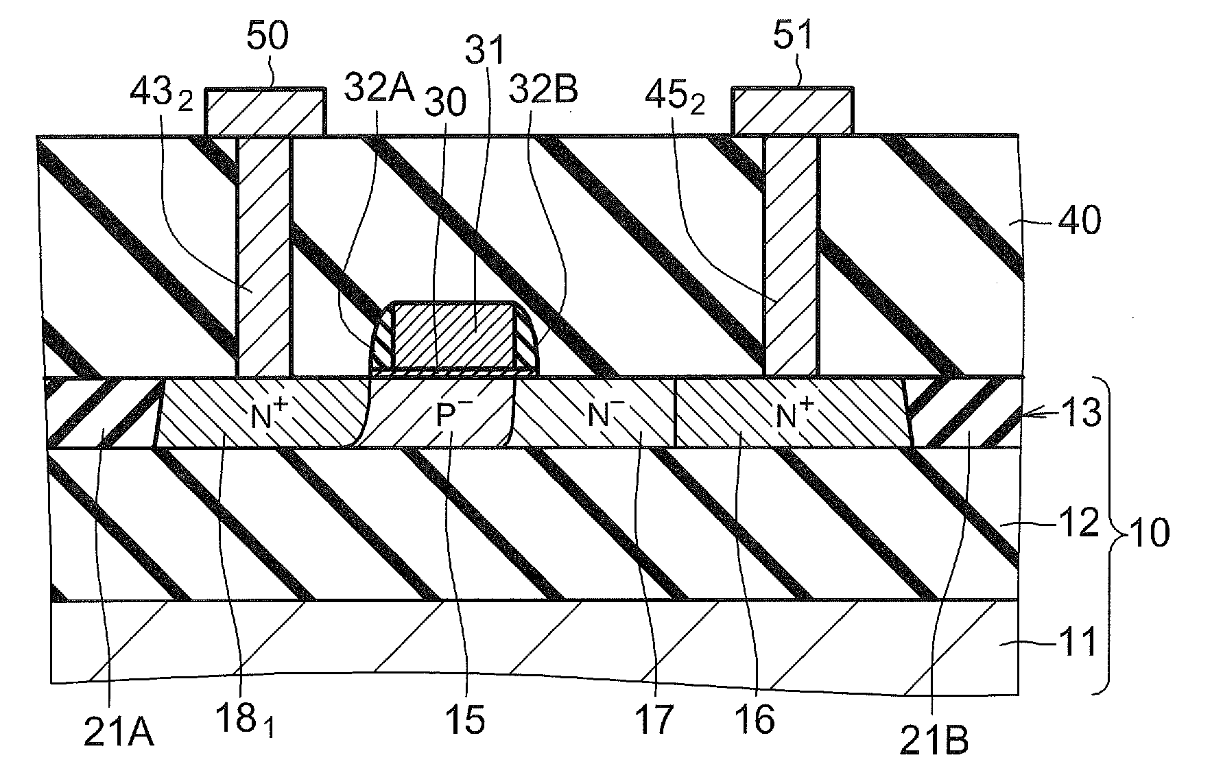
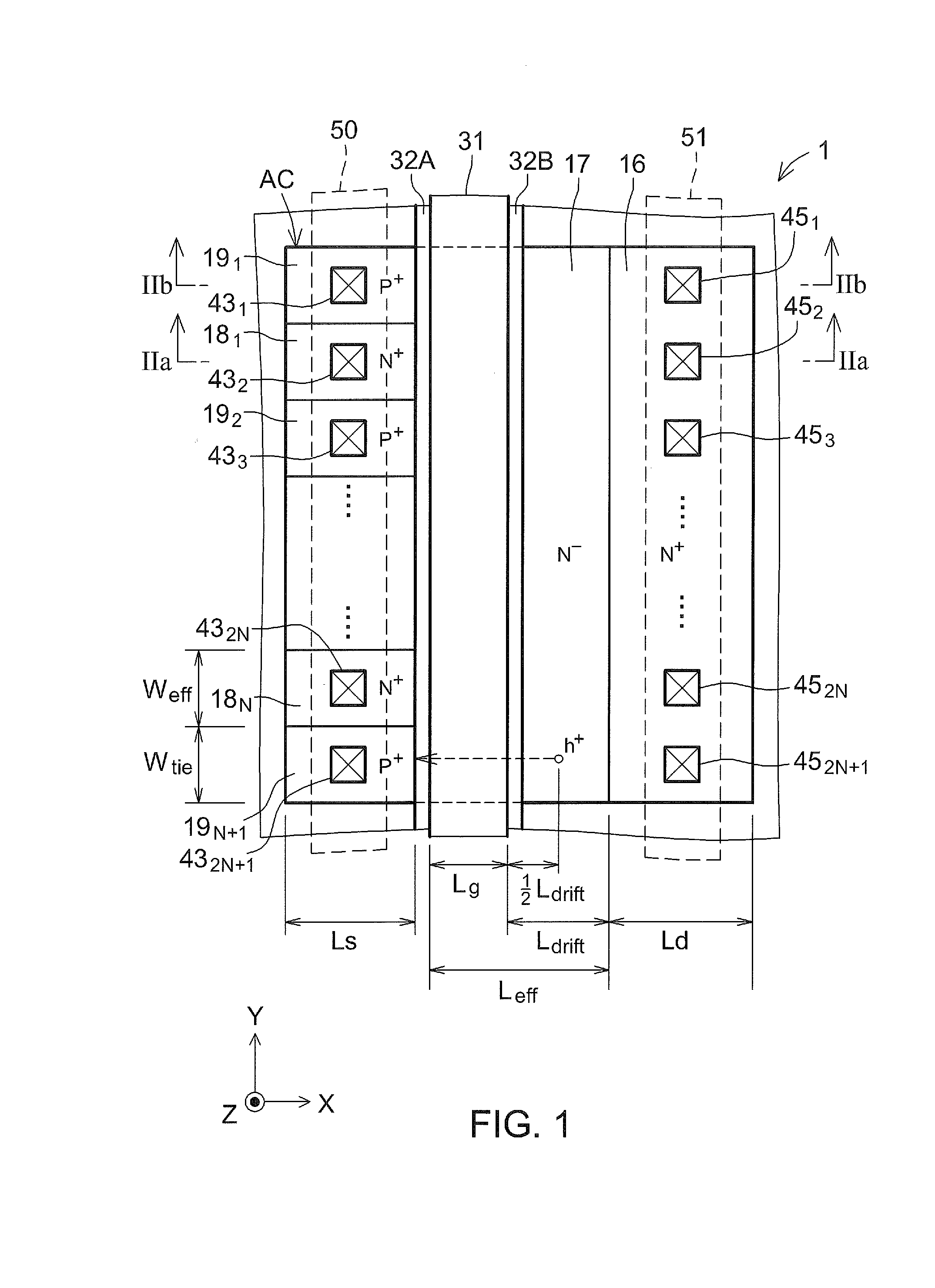
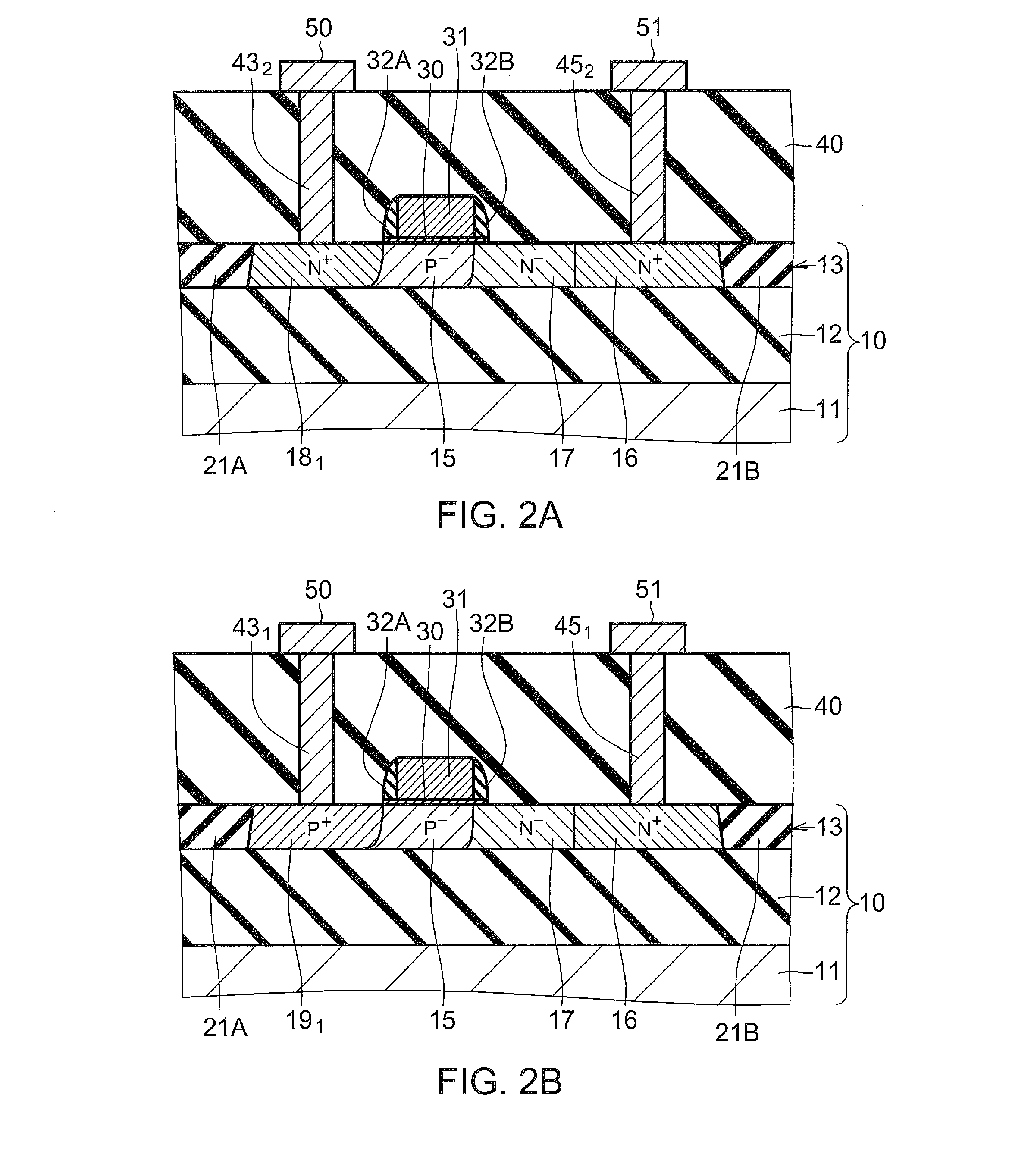
[0028]The embodiment is a semiconductor device 1 with the structure partially shown in FIGS. 1, 2A, and 2B. In the Cartesian coordinate system shown in FIG. 1, the Y-axis indicates the first direction and the X-axis indicates the second direction. FIGS. 2A and 2B both illustrate sections parallel to the X-Z plane.

[0029]The semiconductor device 1 includes both power and logic circuit sections all formed on the same SOI substrate 10. FIGS. 1, 2A, and 2B show the structure of one power circuit element in the power circuit section. The illustrated circuit element has an N-channel metal-oxide-semiconductor (NMOS) field-effect transistor structure.

[0030]As shown in FIGS. 2A and 2B, the SOI substrate 10 includes a base layer 11, a buried insulating layer 12 disposed on the base layer 11, and a semiconductor layer 13 disposed o...


PUM


Abstract

A semiconductor device formed on a silicon-on-insulator substrate includes a gate electrode, a gate insulation film, a drain diffusion region, a drift region, a body region, a plurality of source diffusion regions, and a plurality of charge collection diffusion regions. The source diffusion regions and charge collection diffusion regions are of mutually opposite conductivity types, and alternate with one another in the direction paralleling the width of the gate electrode. The half-width of each source diffusion region is equal to or less than the length of the gate electrode plus the half-length of the drift region.

Description

BACKGROUND OF THE INVENTION[0001]1. Field of the Invention[0002]The present invention relates to a semiconductor device, more particularly a semiconductor-on-insulator device including a field-effect transistor, and to its fabrication method.[0003]2. Description of the Related Art[0004]Energy conservation and power efficiency are demanded in modern electrical and electronic devices, including consumer devices, automotive devices, and lighting devices. Light emitting diode (LED) illumination, photovoltaic power generation, and power management, in which power is supplied to only the necessary operational blocks in an electrical or electronic device, are among the technologies being developed to meet these demands. There are also demands for greater power efficiency and smaller size in the field of power electronics, particularly regarding the metal-oxide-semiconductor field-effect transistors (MOSFETs) that consume large amounts of power in power electronics circuits. A recent trend ...

Claims


Application Information

Patent Timeline
Patent Type & Authority Applications(United States)
IPC IPC(8): H01L29/78
CPCH01L29/78615H01L29/0692H01L29/78624H01L29/7824H01L29/66681H01L29/1095
Inventor MIURA, NORIYUKI
Owner LAPIS SEMICON CO LTD
Why Eureka
Try Eureka