Resistive ladder, summing node circuit, and trimming method for a subranging analog to digital converter

a technology of resistive ladder and resistive node, applied in the field of electronic devices, can solve the problems of flash adcs providing higher conversion speed, higher input capacitance, and adcs not meeting the needs of the marketpla

Inactive Publication Date: 2005-04-19
MICROELECTRONICS TECH INC
View PDF6 Cites 36 Cited by
  • Summary
  • Abstract
  • Description
  • Claims
  • Application Information

AI Technical Summary

Problems solved by technology

Flash ADCs provide higher speed of conversion, but are limited by higher input capacitance, power consumption, and device yield constraints associated with the high number of comparators in the circuitry.
Currently available ADCs do not meet the needs of the marketplace.
In the prior art quantizer, the current sources are employed as current sinks, which loads down the hold amplifier driving the quantizer and requires too much power.
This design dissipates too much power, plus the offset current sources are noisy and bandlimited, which creates settling problems with the offset currents.
Furthermore, subranging ADCs may exhibit significant nonlinearity errors that tend to repeat in response to an analog input signal.
Because the spurs tend to lie very close to the signal frequency, it is difficult and expensive to remove them using conventional filtering techniques.

Method used


Image

  • Resistive ladder, summing node circuit, and trimming method for a subranging analog to digital converter
  • Resistive ladder, summing node circuit, and trimming method for a subranging analog to digital converter
  • Resistive ladder, summing node circuit, and trimming method for a subranging analog to digital converter

Examples


Embodiment Construction

[0025]Illustrative embodiments and exemplary applications will now be described with reference to the accompanying drawings to disclose the advantageous teachings of the present invention.

[0026]While the present invention is described herein with reference to illustrative embodiments for particular applications, it should be understood that the invention is not limited thereto. Those having ordinary skill in the art and access to the teachings provided herein will recognize additional modifications, applications, and embodiments within the scope thereof and additional fields in which the present invention would be of significant utility.

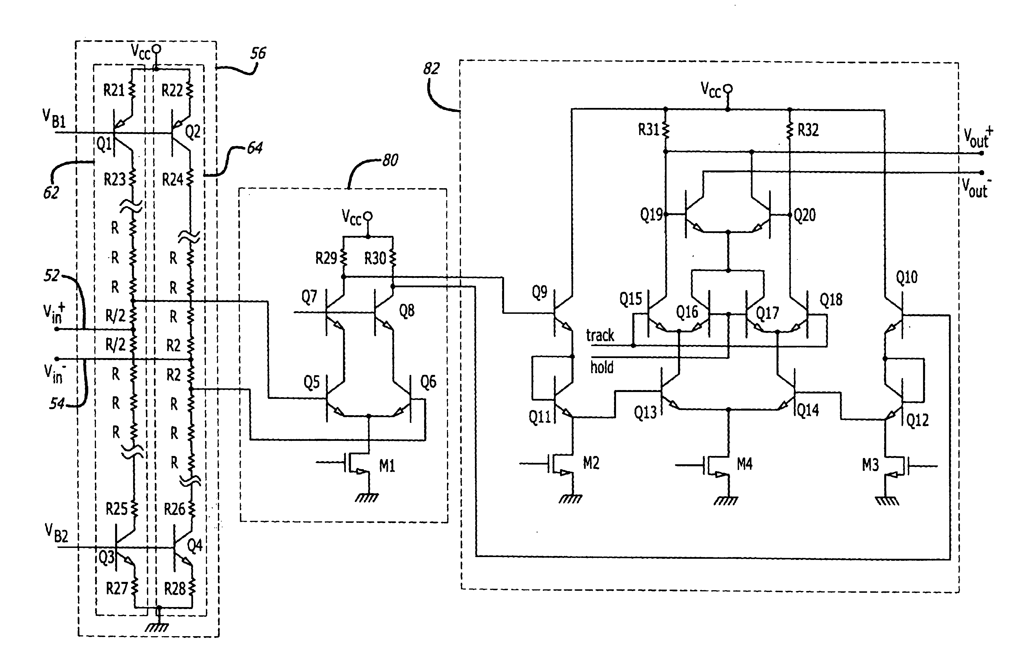
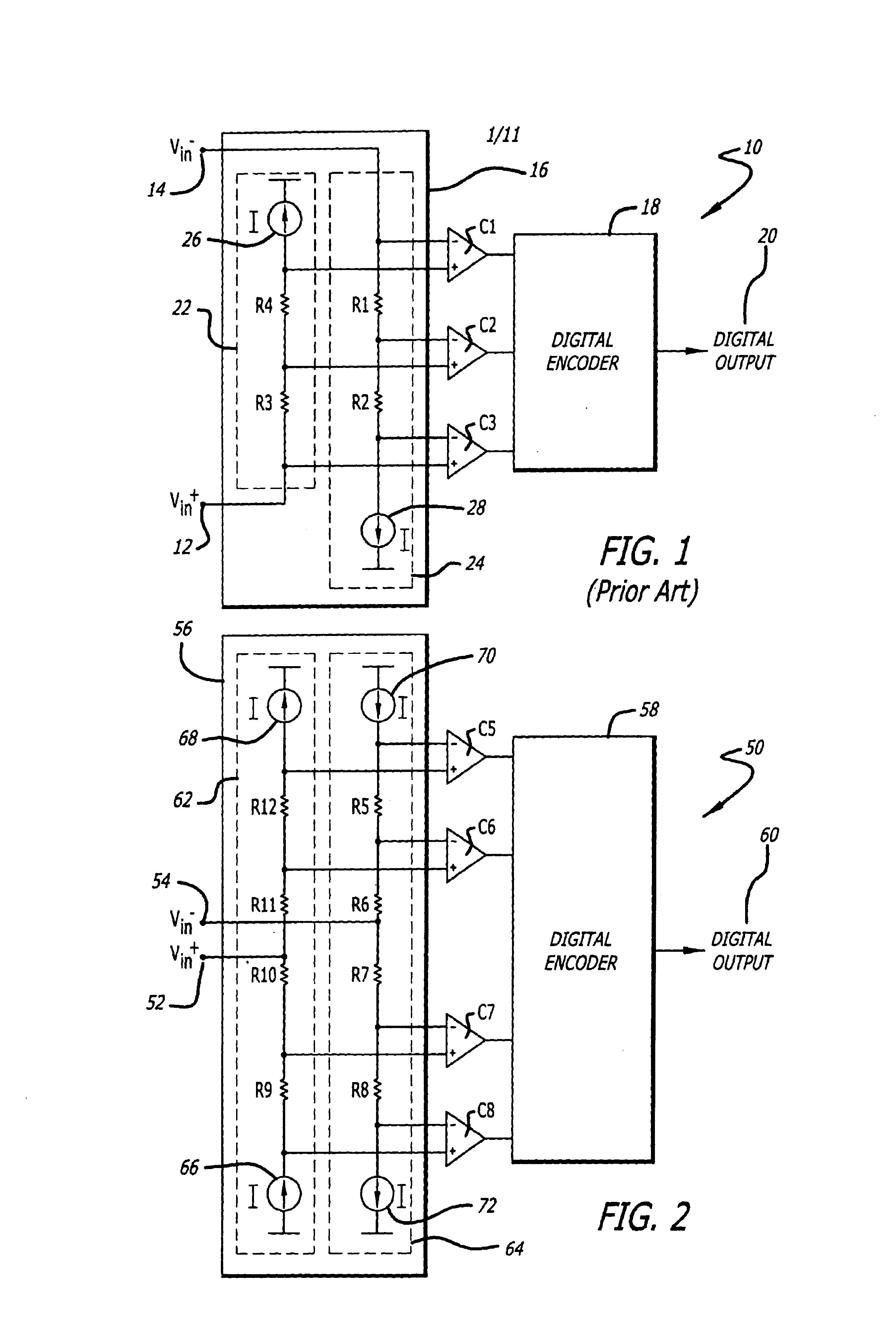
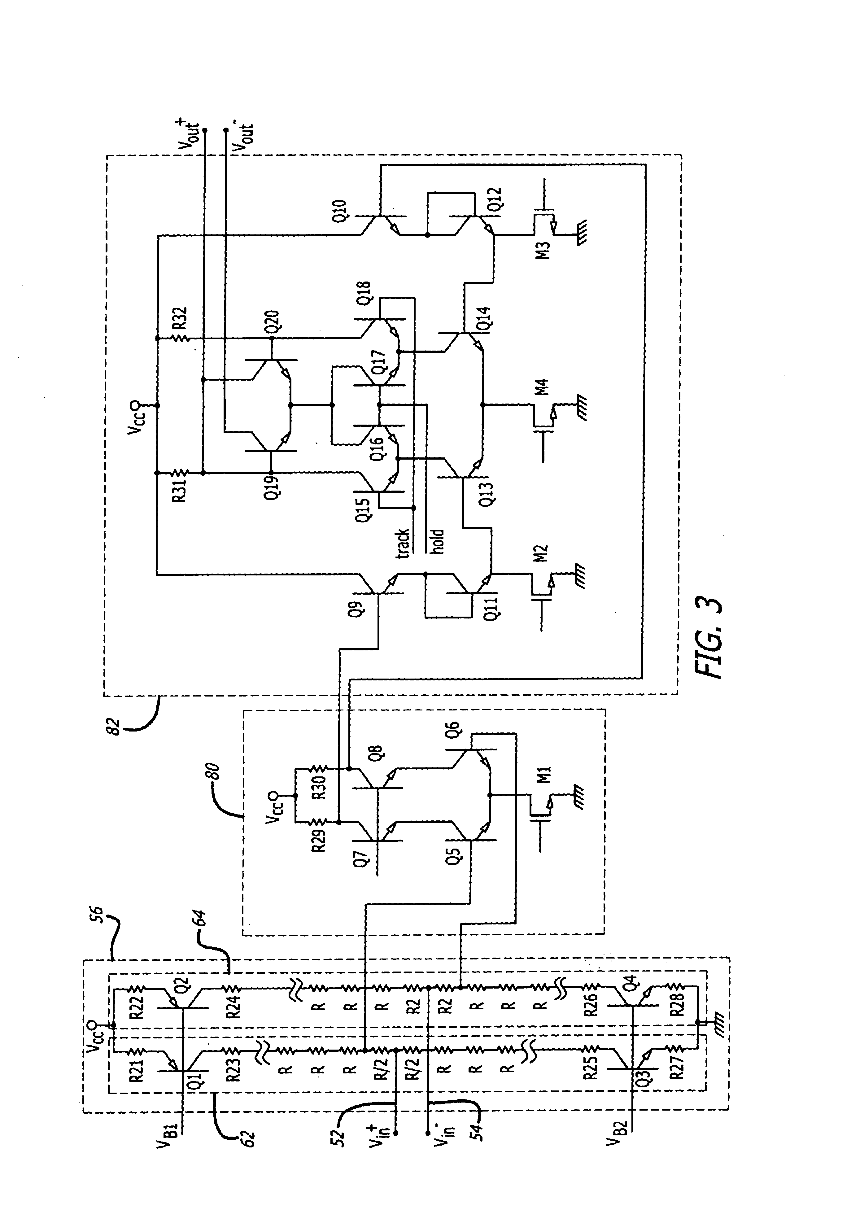
[0027]In order to reduce the power of the ADC IC, new circuit architectures are required to be developed that take advantage of present day process technologies. Specifically, present day BiCMOS, or complementary bipolar, or CBiCMOS, can be utilized to reduce the power associated with the flash quantizer structure and the summing node circuit. Comple...


PUM


Abstract

A subranging analog to digital converter (ADC). The ADC (200) includes a novel resistive ladder (56) for a differential quantizer (50) and a novel summing node circuit (150). The novel resistive ladder (56) includes an input terminal (52), a plurality of serially connected resistors R coupled to the input terminal (52), and a pair of complementary current sources (66 and 68) for maintaining a constant current flow through the ladder (56). The novel summing node circuit (150) includes an input terminal (152) for receiving an input signal, a pair of complementary DACs (156 and 158) for generating a reconstruction signal, and a summing amplifier (164) for subtracting the reconstruction signal from the input signal to produce a residue signal.The invention also includes a method for trimming the subranging ADC. The novel method (250) includes the steps of trimming the complementary current sources of the coarse quantizer to match each other (252), trimming each of the DAC cells on one of the complementary DACs (254), trimming the overall DAC gain to match the gain of the coarse quantizer (256); and trimming the gain of the fine quantizer to match one coarse quantization Q level (260).

Description

BACKGROUND OF THE INVENTION[0001]1. Field of the Invention[0002]The present invention relates to electronics. More specifically, the present invention relates to analog to digital converters.[0003]2. Description of the Related Art[0004]The function of an analog to digital converter (ADC) is to accurately convert an analog input signal into a digital output represented by a coded array of binary bits. The output bits are generated by processing the analog input signal through a number of comparator steps. An N-bit digital output can be produced in one step with 2N-1 parallel comparators (flash ADCs) or, at the limit, by N sequential steps with a single comparator (successive approximation ADCs). Flash ADCs provide higher speed of conversion, but are limited by higher input capacitance, power consumption, and device yield constraints associated with the high number of comparators in the circuitry. At the other extreme, successive approximation ADCs are simple in structure, and may be ...

Claims


Application Information

Patent Timeline
Patent Type & Authority Patents(United States)
IPC IPC(8): H03M1/36H03M1/78H03M1/74H03M1/06H03M1/10H03M1/16
CPCH03M1/0682H03M1/1057H03M1/747H03M1/363H03M1/167
Inventor LINDER, LLOYD F.FELDER, BENJAMIN
Owner MICROELECTRONICS TECH INC
Why Eureka
Try Eureka