Method of manufacturing semiconductor local interconnect and contact

a local interconnect and contact technology, applied in the field of integrated circuits, can solve the problems of increasing the complexity of metalization, shortening the process window for etching openings, and increasing the complexity of integrated circuits, so as to prevent the formation of keyholes

Inactive Publication Date: 2005-04-26
CHARTERED SEMICONDUCTOR MANUFACTURING
View PDF7 Cites 234 Cited by
  • Summary
  • Abstract
  • Description
  • Claims
  • Application Information

AI Technical Summary

Benefits of technology

[0012]The present invention provides for a method of manufacturing an integrated circuit with a semiconductor substrate having a first gate dielectric and a first gate provided thereon and thereover. A lightly doped drain is formed in the semiconductor substrate adjacent the gate dielectric, and a spacer liner is formed on the substrate around the first gate dielectric and the first gate. A first spacer is formed on the spacer liner and around the first gate. A second spacer is formed on the first spacer and around the first gate. A first dielectric layer is formed over the semiconductor substrate, the spacer liner, the first and second spacers, and the first gate. A second dielectric layer is formed over the first dielectric layer. A local interconnect opening is formed in the second dielectric layer down to the first dielectric layer. The local interconnect opening in the first dielectric layer is opened to expose the junction in the semiconductor substrate and the first gate. The local interconnect openings in the first and second dielectric layers are filled with a conductive material. The method prevents gouging of the shallow trench isolations and loss of isolating spacers while preventing the formation of keyholes.

Problems solved by technology

As the complexity of integrated circuit is increased, the complexity of metalization has also increased.
There are a number of problems with existing processes such as those caused by larger openings etching at a different rate than smaller openings.
Further, the process window for time for etching openings becomes very short when trying to create the different sized isolated contacts and local interconnects.
In these cases, the processes often result in gouging of the shallow trench isolations, which separate the semiconductor devices, and loss of isolating spacers.
Also, incomplete filling results in a void area, also known as a “keyhole,” that is formed within the metalization.
This keyhole is detrimental because it can open up during further processing steps, where material which could corrode or corrupt the tungsten layer can make its way into the keyhole.
Solutions to problems of this sort have been long sought, but there has been no teaching or suggestion in the prior art how those having ordinary skill in the art could solve these problems.

Method used


Image

  • Method of manufacturing semiconductor local interconnect and contact
  • Method of manufacturing semiconductor local interconnect and contact
  • Method of manufacturing semiconductor local interconnect and contact

Examples


Embodiment Construction

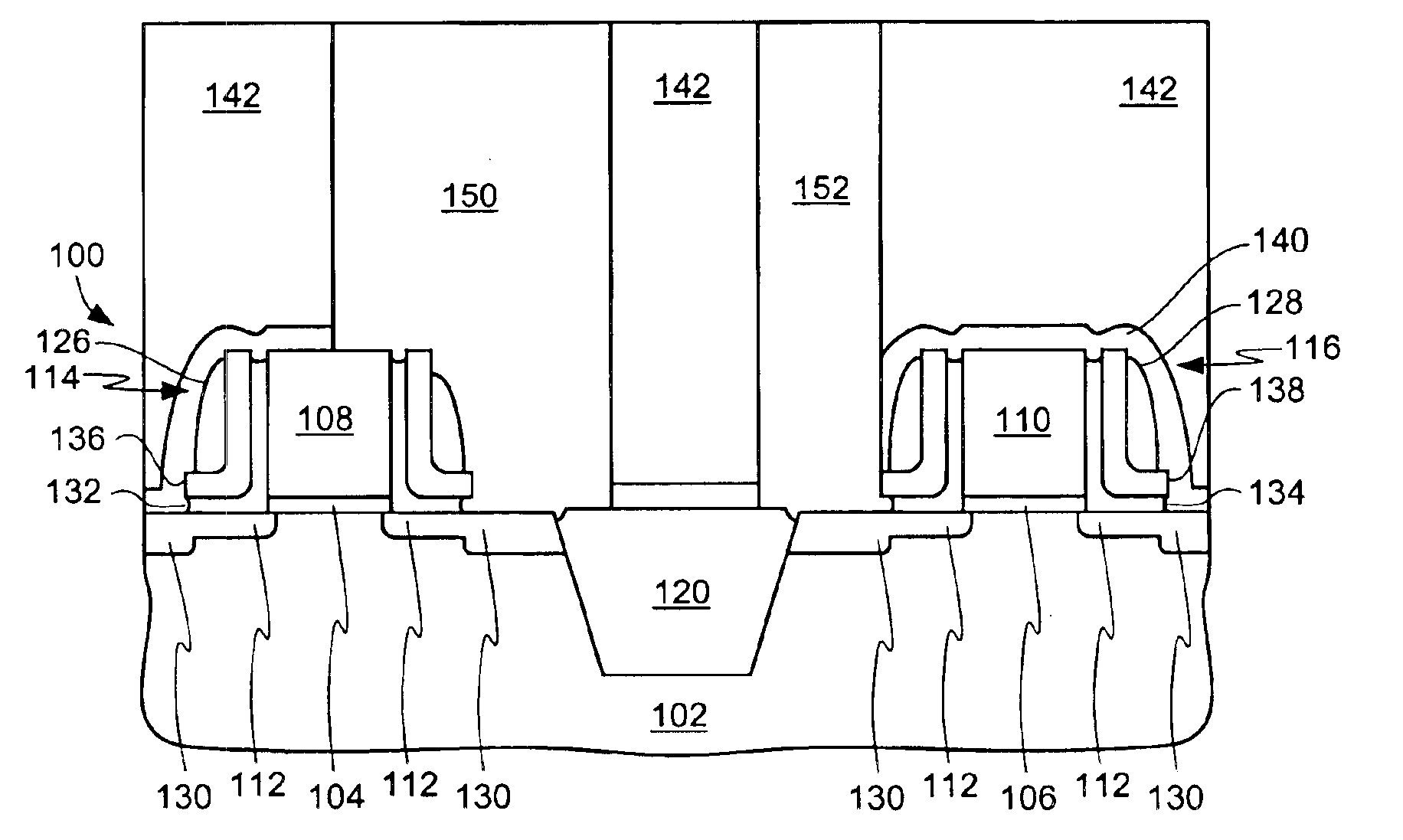
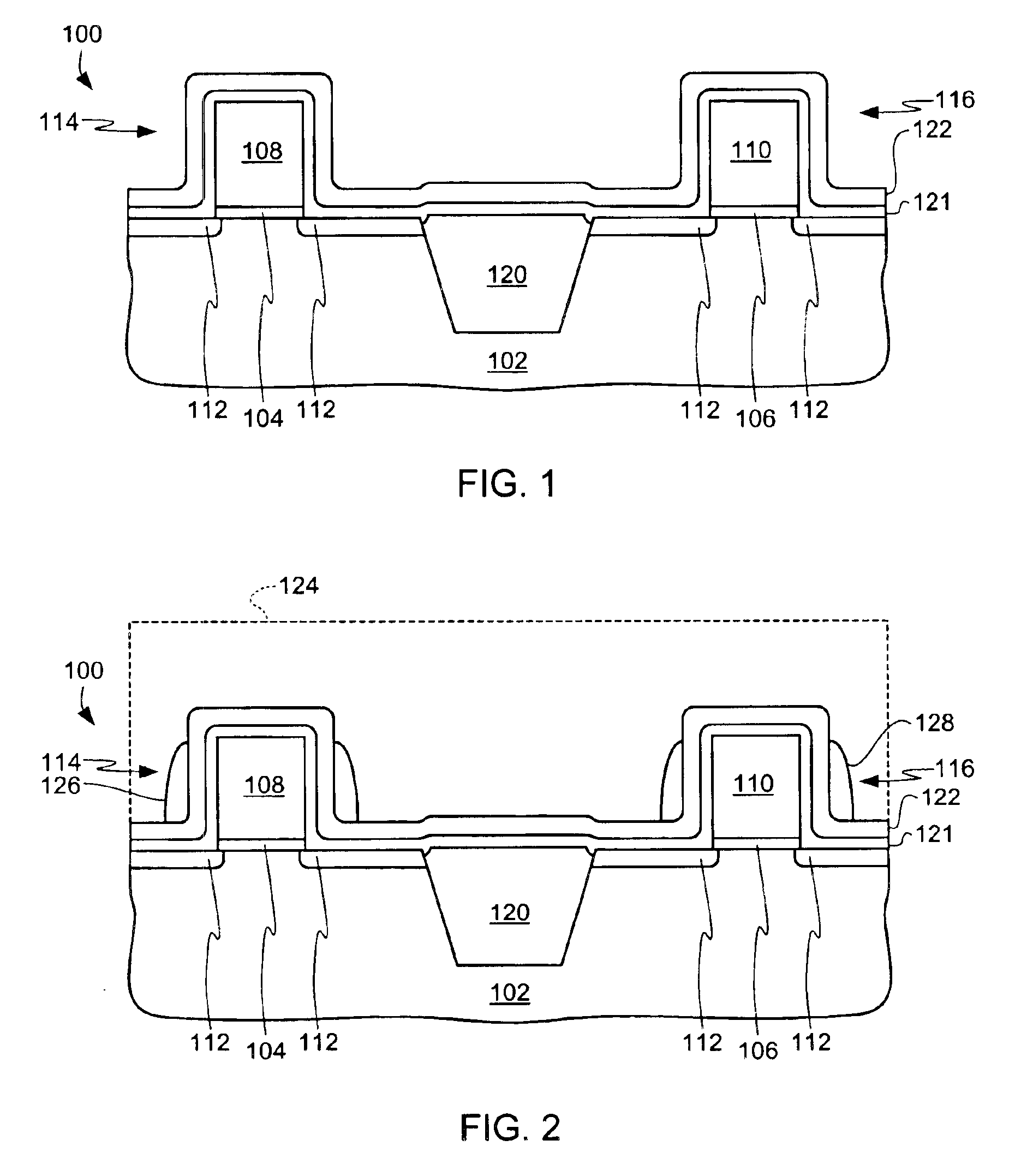
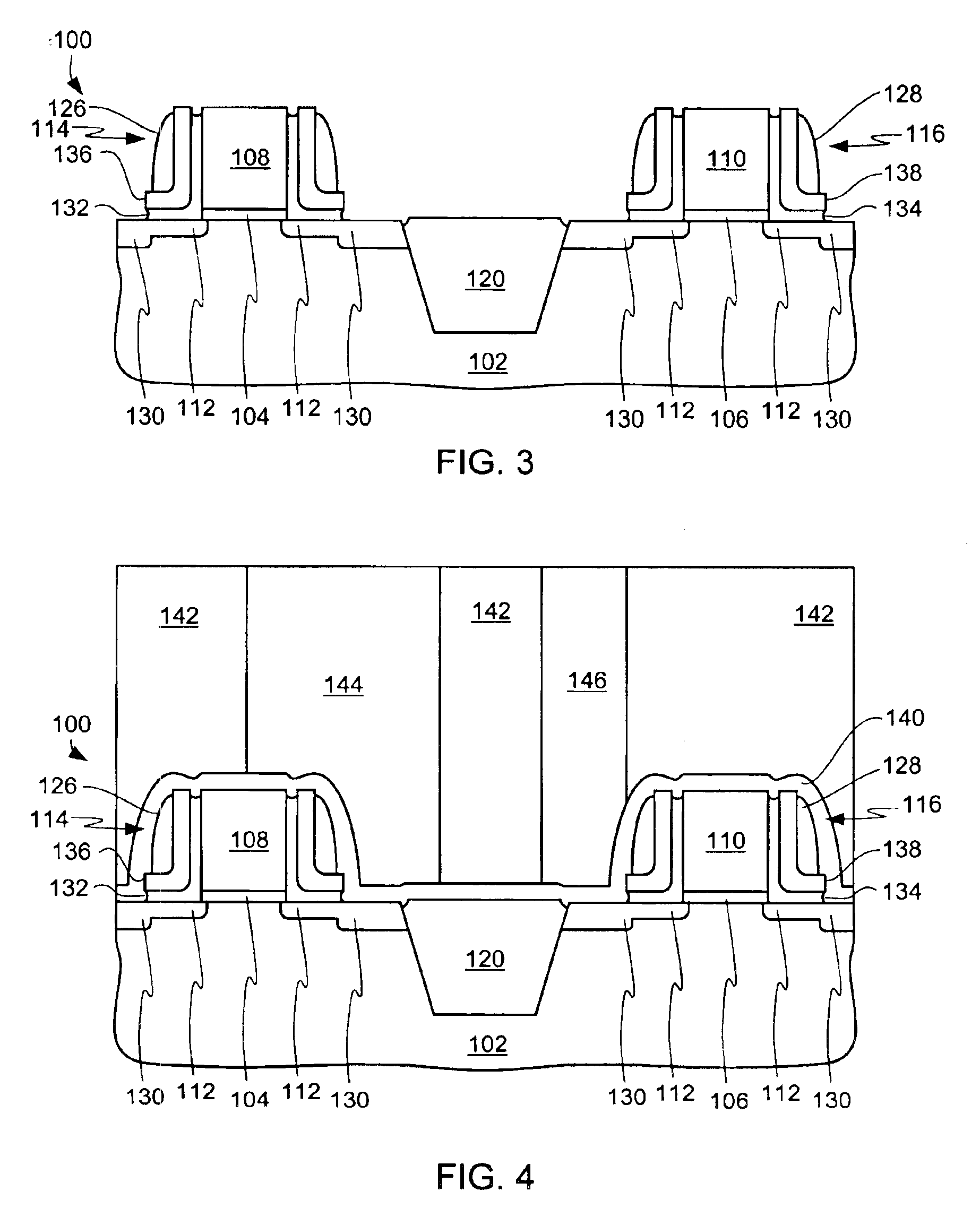
[0020]Referring now to FIG. 1, therein is shown an integrated circuit 100 in an intermediate stage of manufacture. The integrated circuit 100 includes a semiconductor substrate 102 having first and second gate dielectrics 104 and 106 formed on the surface of the semiconductor substrate 102 under first and second semiconductor gates 108 and 110, respectively.

[0021]The term “horizontal” as used in herein is defined as a plane parallel to the conventional plane or surface of a wafer or substrate, regardless of its orientation. The term “vertical” refers to a direction perpendicular to the horizontal as just defined. Terms, such as “on”, “above”, “below”, “side” (as in “sidewall”), “higher”, “lower”, “over”, and “under”, are defined with respect to the horizontal plane. The term “processing” as used herein includes deposition of material or photoresist, patterning, exposure, development, etching, cleaning, and / or removal of the material or photoresist as required in forming a described ...


PUM


Abstract

An integrated circuit, and manufacturing method therefor, is provided. A gate dielectric and a gate are provided respectively on and over a semiconductor substrate. A junction is formed adjacent the gate dielectric and a shaped spacer is formed around the gate. A spacer is formed under the shaped spacer and a liner is formed under the spacer. A first dielectric layer is formed over the semiconductor substrate, the shaped spacer, the spacer, the liner, and the gate. A second dielectric layer is formed over the first dielectric layer. A local interconnect opening is formed in the second dielectric layer down to the first dielectric layer. The local interconnect opening in the first dielectric layer is opened to expose the junction in the semiconductor substrate and the first gate. The local interconnect openings in the first and second dielectric layers are filled with a conductive material.

Description

BACKGROUND[0001]1. Technical Field[0002]The present invention relates generally to integrated circuits, and more specifically to local interconnects and isolated contacts for interconnecting semiconductor devices.[0003]2. Background Art[0004]As semiconductor technology continues to evolve, a continuing trend is towards ultra large-scale integration with the fabrication of smaller and smaller integrated circuits with more and faster semiconductor devices.[0005]Fabrication of an integrated circuit involves numerous processing steps. After doped regions have been deposited to form source / drain junctions within a semiconductor substrate and gates have been defined on the substrate, dielectric layers are deposited on the semiconductor devices and conductors are routed over the dielectric layers to connect to and fill openings formed through the dielectric layer to the source / drain junctions and gates. The entire process of routing and making connections is generally termed “metalization”...

Claims


Application Information

Patent Timeline
Patent Type & Authority Patents(United States)
IPC IPC(8): H01L21/336H01L21/60H01L21/768H01L21/8234
CPCH01L21/76895H01L21/76897H01L21/823468H01L21/823475H01L29/6656
Inventor YELEHANKA, PRADEEPCHEN, TONG QINGHAN, ZHI YONGZHENG, ZHEN JIAONG, KELVINGU, TIAN HAOCHEAH, SYN KEAN
Owner CHARTERED SEMICONDUCTOR MANUFACTURING
Why Eureka
Try Eureka