MOS transistor device with a locally maximum concentration region between the source region and the drain region

a technology of mos transistor and drain region, which is applied in the direction of semiconductor devices, semiconductor/solid-state device details, electrical devices, etc., can solve the problem of low resistance of mos transistor devices, and achieve the effect of low resistan

Inactive Publication Date: 2005-04-26
INFINEON TECH AG
View PDF10 Cites 21 Cited by
  • Summary
  • Abstract
  • Description
  • Claims
  • Application Information

AI Technical Summary

Benefits of technology

[0005]It is accordingly an object of the invention to provide a MOS transistor device that overcomes the above-mentioned disadvantages of the pr

Problems solved by technology

The MOS transistor device contains a semiconductor region having a trench structure formed therein extending substantially in a given direction, and an avalanche breakdown region formed i

Method used


Image

  • MOS transistor device with a locally maximum concentration region between the source region and the drain region
  • MOS transistor device with a locally maximum concentration region between the source region and the drain region
  • MOS transistor device with a locally maximum concentration region between the source region and the drain region

Examples


Embodiment Construction

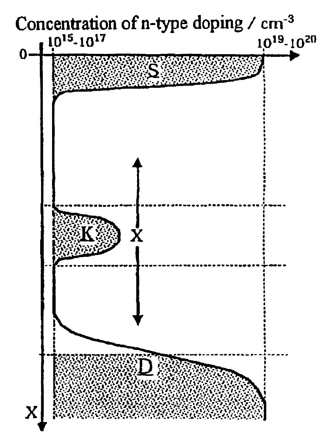
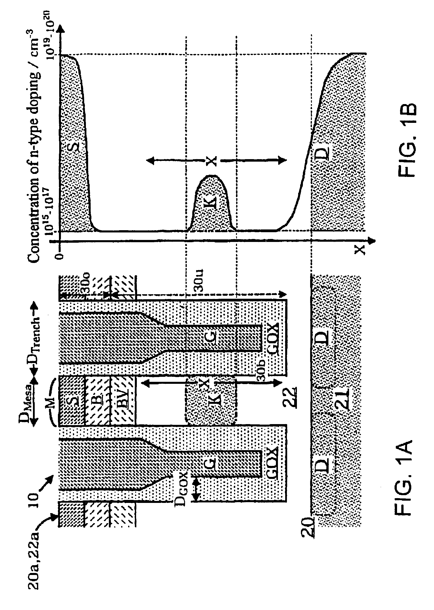
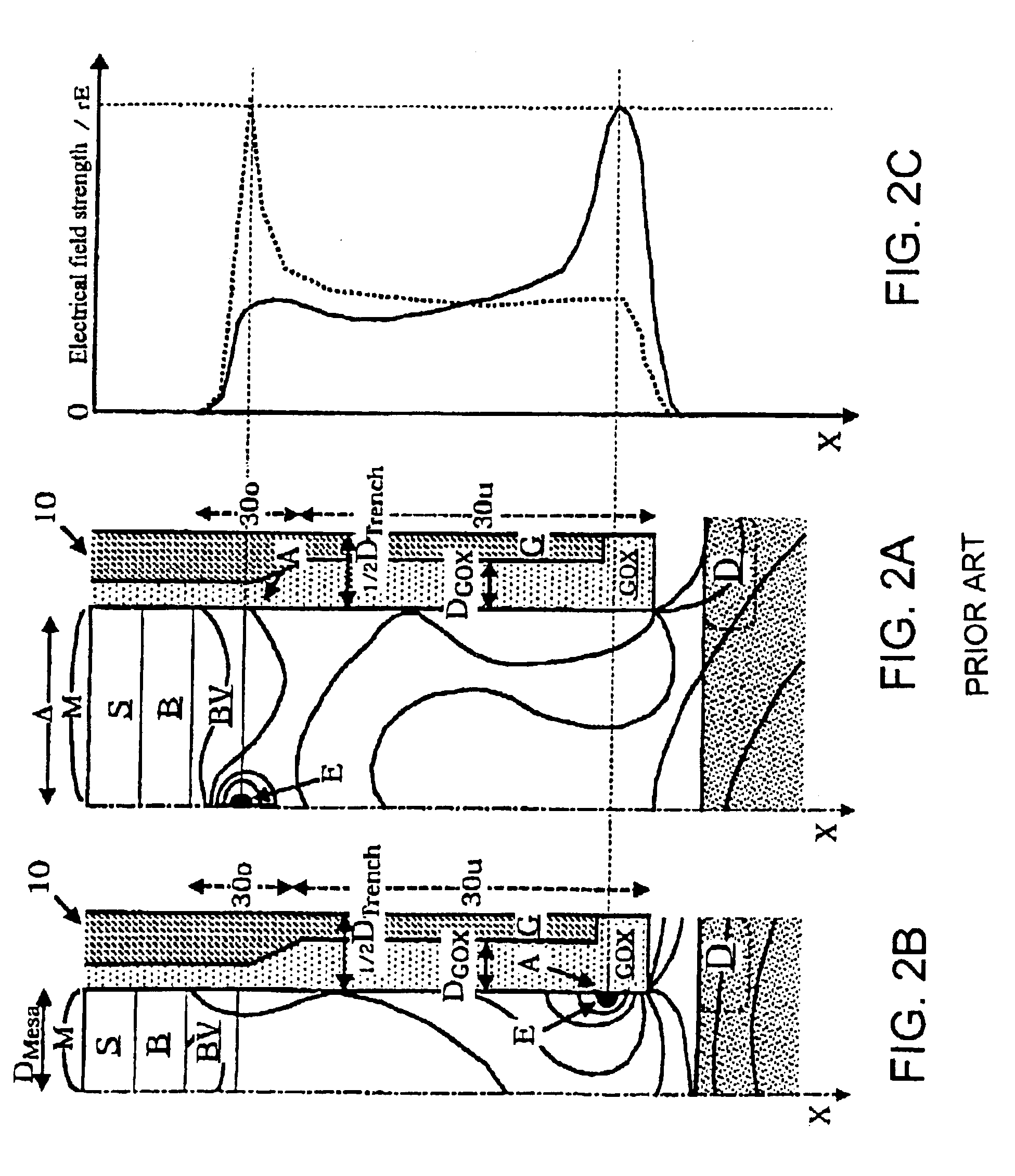
[0047]Referring now to the figures of the drawing in detail and first, particularly, to FIG. 1A thereof, there is shown in lateral cross-sectional view of a semiconductor circuit configuration having two MOS transistor devices 10 formed according to the invention.

[0048]The MOS transistor devices 10 formed according to the invention are formed in a semiconductor region 20 such that they are adjacent to one another in a manner isolated by a mesa region M having a thickness DMesa, to be precise in a semiconductor subregion 22 thereof which is essentially initially at most lightly doped. Each MOS transistor device 10 formed according to the invention has a trench 30 or a trench structure 30 having a width DTrench.

[0049]The wall regions of the trench structures 30 are lined with a gate oxide GOX serving as an insulation region GOX. The gate oxide GOX has a maximum thickness DGOX in a lower region 30u or end region 30u of the trench structure 30. The gate oxide GOX is made much narrower i...


PUM


Abstract

In order to obtain an on resistance that is as low as possible, it is proposed, in the case of a MOS transistor device, to form the avalanche breakdown region in an end region of a trench structure. As an alternative or in addition, it is proposed to form a region of local maximum dopant concentration of a first conductivity type in the region between a source and a drain in proximity to the gate insulation in a manner remote from the gate electrode.

Description

BACKGROUND OF THE INVENTIONField of the Invention[0001]The invention relates to a MOS transistor device having a trench structure extending substantially in a first direction in the semiconductor region.[0002]In modern MOS transistors, in particular in the power semiconductor field, an essential criterion in assessing the function is the on resistance of the respective MOS transistor device.[0003]The further development of modern transistor technologies often aims to reduce the on resistivity, so that the static power loss can be minimized and larger current densities can be achieved, thus resulting in the possibility of miniaturization of the chips in conjunction with cost-effective production.[0004]Known measures for reducing the on resistivity of MOS transistors use, instead of a planar cell structure, trench cells in which the MOS transistor is formed in the region of a trench or trench structure which accommodates the gate electrode and the gate terminal. By virtue of this meas...

Claims


Application Information

Patent Timeline
IPC IPC(8): H01L29/66H01L29/78H01L29/02H01L29/08H01L29/423H01L29/10H01L29/40
CPCH01L29/7813H01L29/0847H01L29/42368H01L29/1095H01L29/0878
Inventor ZUNDEL, MARKUSHIRLER, FRANZLANTIER, ROBERTA
Owner INFINEON TECH AG
Why Eureka
Try Eureka