Method and apparatus for thickness decomposition of complicated layer structures

a layer structure and thickness decomposition technology, applied in the direction of instruments, semiconductor/solid-state device testing/measurement, fluorescence/phosphorescence, etc., can solve the problems of reducing the actual production time using the machine, and consuming additional raw materials,

Active Publication Date: 2005-04-26
ONTO INNOVATION INC
View PDF6 Cites 75 Cited by
  • Summary
  • Abstract
  • Description
  • Claims
  • Application Information

AI Technical Summary

Benefits of technology

[0080]Preferably, the measuring units are located to take thickness measurements before, during and af

Problems solved by technology

The above methods have limitations when used in the production line.
The special run that is needed to produce the test sample has the effect of reducing actual production time using the machines and consumes additional raw materials.
On the other hand measuring actual production units using the alignment technique takes time, requires sophisticated h

Method used


Image

  • Method and apparatus for thickness decomposition of complicated layer structures
  • Method and apparatus for thickness decomposition of complicated layer structures
  • Method and apparatus for thickness decomposition of complicated layer structures

Examples


Embodiment Construction

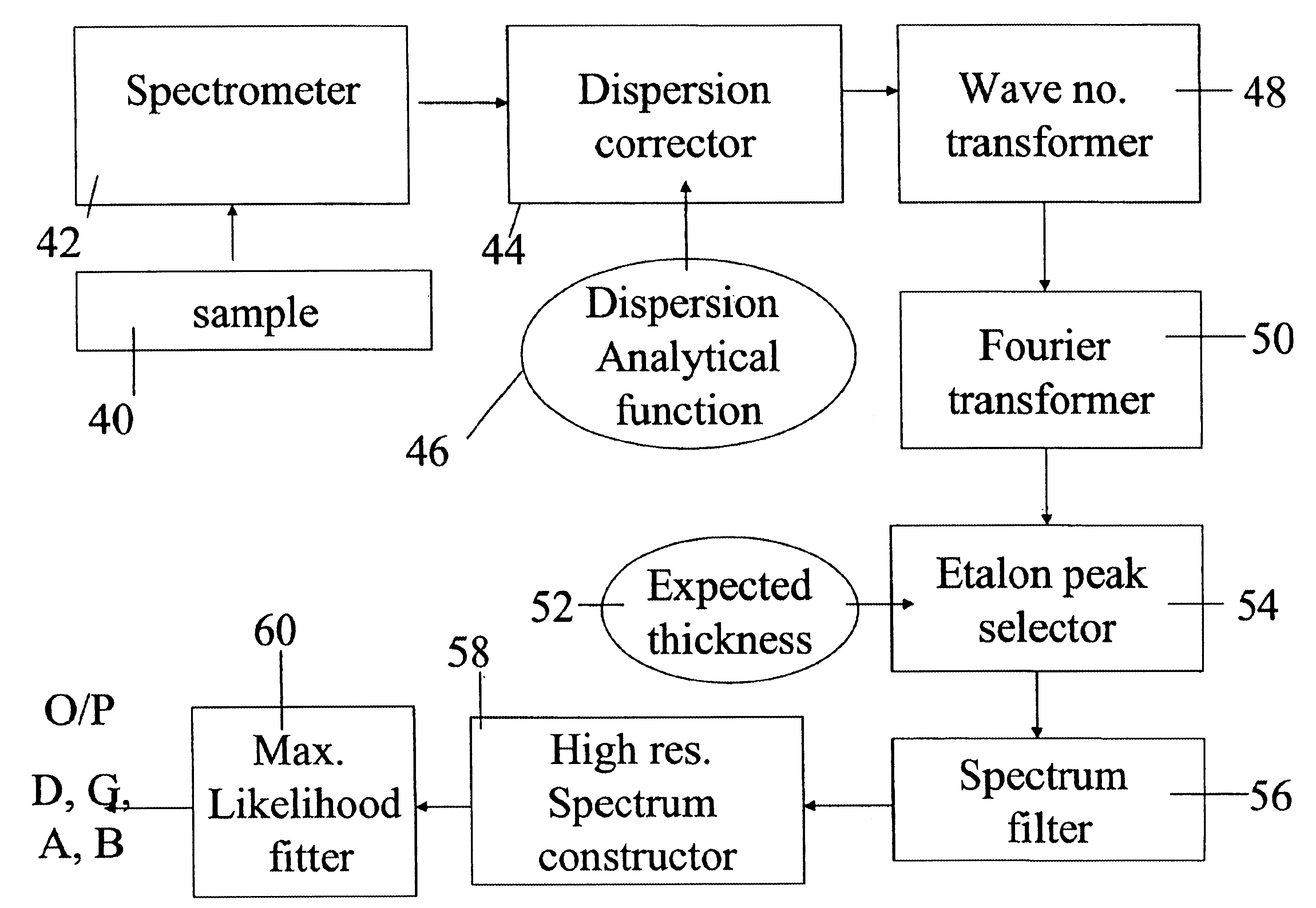
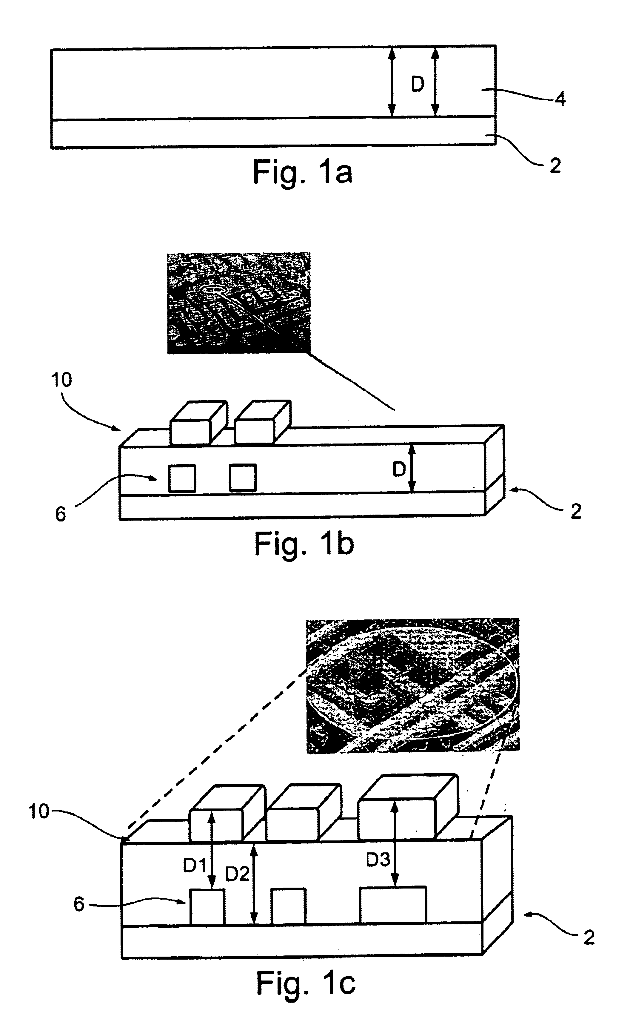
[0094]The present embodiments describe a two-stage system, which uses the TMS system of PCT Patent Application No. WO 0012958, the contents of which are hereby incorporated by reference in their entirety. In the first, learning, stage a TMS-based layer characterization of a typical sample of a semiconductor wafer product is made for a given stage of manufacturing. This stage is carried out as accurately as possible using such techniques as estimation of high resolution spectra than that originally taken. Such techniques are highly calculation intensive and thus not currently suitable for real time processing. The estimation of high-resolution spectrum is used to produce starting points for maximum likelihood fitting. In a second stage, measurements of actual semiconductor products reaching the given stage are taken and deviations of the layer thicknesses vis a vis the sample are determined. The second stage also uses maximum likelihood fitting, however, in the second stage the maxim...


PUM


Abstract

Thickness measurement apparatus for measuring layer thicknesses on patterned areas of a semiconductor wafer, comprises: a spectrum analyzer for obtaining reflection data taken from a patterned area and obtaining therefrom a frequency spectrum, a peak detector for searching the spectrum to find peak frequencies within said spectrum, the search being restricted to regions corresponding to peak frequencies found in an earlier learning stage, a frequency filter, associated with the peak detector, for filtering the spectrum about said peak frequencies, and a maximum likelihood fitter for using parameters obtained in the learning stage to carry out maximum likelihood fitting of said filtered spectrum to obtain the desired layer thicknesses. By carrying out maximum likelihood fitting using parameters obtained beforehand in a high resolution non-real time learning stage, it is possible to provide high resolution results in real time.

Description

FIELD OF THE INVENTION[0001]The present invention relates to a method and apparatus for measuring physical parameters of complicated layer structures.BACKGROUND OF THE INVENTION[0002]The manufacturing process of semiconductor devices and similar products such as flat panel displays, MEMS and memory discs, involves numerous process steps where layers are deposited, etched, coated and abraded by polishing. To control process step performance for each unit running in the production line it is important to monitor the physical parameters of the layers before, during, and after the respective process step. Some of the process steps involve selective etching or deposition of the layers to form patterns on the wafer such as metal lines, dielectric or Si trenches, Photo resist patterns etc.[0003]Methods of measuring the layer thickness are well known and may include amongst others:[0004]Reflectometry where interference between the reflected light from the top surface of the layer and the bo...

Claims


Application Information

Patent Timeline
IPC IPC(8): G01B11/06
CPCG01B11/0625H01L22/00H01L21/31
Inventor DU-NOUR, OFERRUBINSTEIN, VLADIMIR
Owner ONTO INNOVATION INC
Why Eureka
Try Eureka