Circuit and method for calibrating DRAM pullup Ron to pulldown Ron

Inactive Publication Date: 2005-04-26
INTEL CORP
View PDF4 Cites 41 Cited by
  • Summary
  • Abstract
  • Description
  • Claims
  • Application Information

AI Technical Summary

Problems solved by technology
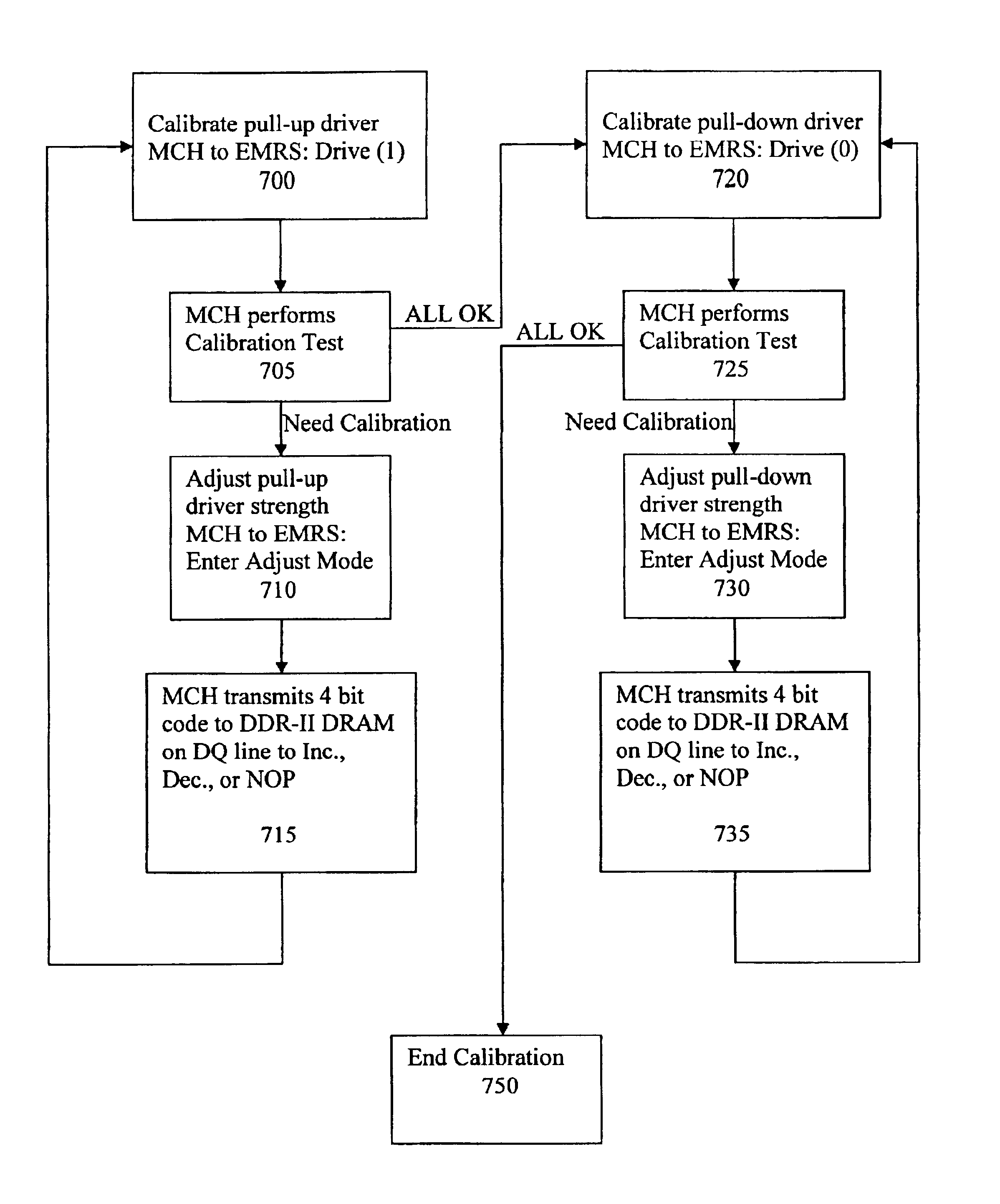
The VREF signal is a high impedance DC voltage reference generated from, and which

Method used


Image

  • Circuit and method for calibrating DRAM pullup Ron to pulldown Ron
  • Circuit and method for calibrating DRAM pullup Ron to pulldown Ron
  • Circuit and method for calibrating DRAM pullup Ron to pulldown Ron

Examples


case 1

[0029, assume a 5% error on resistor tolerances that may be representative of an ASIC process. For example, assuming a 20 ohm resistor and the value of R321 is −2.5% low, R322 is −2.5% low and the value of R323 is +2.5% high. Furthermore, treat Rstub=22 ohms and Rt=20 ohms as ideal.

VrefHi=(R323+R322) / (R321+R322+R323)*(VDDQ−VSS)

VrefHi=[(20.5+19.5) / (20.5+19.5+19.5)]*VDDQ=1.21V

VrefLo=(R323) / (R321+R322+R323)*(VDDQ−VSS)*

 VrefLo=[20.5 / (20.5+19.5+19.5)]*VDDQ=0.62V

Calculating the Calibration error gives:

Vn=VrefHi

Ical=(Vn−Vtt) / Rt=(1.21−0.9) / 20=15.5 mA

Vy=Ical*(Rt+Rstub)=16*(20+22)+Vtt=1.55V

Vds=VDDQ−Vy=1.8−1.55=0.25

RonP=Vds / Ical=0.25 / 0.0155=16.1 ohm vs. a target of 18 ohms.

So, the calibration error term is 11% for the P driver.

Calculating the N driver error:

Vn=VrefLo

Ical=(Vtt−Vt) / Rt=(0.9−0.62) / 20=14 mA

Vy=Ical*(Rt+Rstub)=14*(20+22)=0.312V

RonN=0.312 / 0.014=22.28 ohm vs. a target of 18 ohms.

Resultant N driver calibration error term is 23%.

[0030]As shown above, the tolerances of the resistors may l...


PUM


Abstract

Embodiments of the present invention enable the matching of pull-up and pull-down driver strengths of a slave device (DDRII SDRAM), i.e., the P-channel/N-channel driver pull-up/pull-down Ron and also calibrates the P-channel/N-channel pull-up/pull-down drivers in their linear region of operation. Specifically, embodiments of the present invention may use the DDR-II Off Chip Driver (OCD) protocol for calibration, in addition to using circuit techniques to calibrate the slave driver pull-up Ron within 1 LSB of the pull-down Ron.

Description

BACKGROUND OF THE INVENTION[0001]1. Field of the Invention[0002]The present invention relates to a semiconductor memory device and a semiconductor memory device calibration method and, more particularly, to a double data rate synchronous dynamic random access memory (DDR SDRAM) and a calibration method therefor.[0003]2. Discussion of the Related Art[0004]Double Data Rate (DDR) memory devices use source synchronous transfers when data is written to or read from the memory devices. The data strobe signal (DQS) is sent along with the data (DQ) to be clocked to a memory controller. The DQS signal is edge-aligned with the DQ signal for read cycles and center-aligned with the DQ signal for write cycles.[0005]Second generation Double Data Rate (DDR-II) devices as defined by JEDEC Solid State Technology Association Standard JESD90 conform to the Series Stub Terminated Logic for 1.8 volt operation (SSTL—1.8) signaling level standard as defined by JEDEC Standard JESD8-15. The SSTL—1.8 standar...

Claims


Application Information

Patent Timeline
IPC IPC(8): G01R31/28G01R31/317G01R35/00G11C29/02
CPCG01R31/31703G01R31/3172G01R35/00G11C29/028G11C29/02G11C29/022G11C11/401
Inventor SALMON, JOSEPH H.TO, HING Y.
Owner INTEL CORP
Why Eureka
Try Eureka