Low-power, low-area power headswitch

a power head and low-area technology, applied in the field of circuits, can solve the problems of increasing the delay of transistors, reducing the power of transistors, so as to improve the performance, improve the mobility of n-channel fet, and reduce the leakage curren

Active Publication Date: 2005-01-13
QUALCOMM INC
View PDF12 Cites 39 Cited by
  • Summary
  • Abstract
  • Description
  • Claims
  • Application Information

AI Technical Summary

Benefits of technology

A low-power, low-area headswitch having improved performance over the conventional P-FET headswitch is provided herein. The inherent higher (electron) mobility of N-channel FET (N-FET) devices over P-FET devices is exploited to implement an N-FET headswitch having less leakage current, lower ON resistance, and smaller device size than for a P-FET headswitch.

Problems solved by technology

For complementary metal oxide semiconductor (CMOS) technology, which is widely used for digital circuits and some analog circuits, a major issue with shrinking transistor size is standby power.
A smaller transistor geometry results in higher electric field (E-field), which stresses a transistor and causes oxide breakdown.
Unfortunately, the lower power supply voltage also increases the delay of the transistors, which is undesirable for high-speed circuits.
However, the lower threshold voltage and smaller transistor geometry result in higher leakage current (or standby current), which is the current passing through a transistor when it is turned off.
Leakage current becomes more problematic as CMOS technology scales smaller.
Leakage current consumes power and reduces standby time for a portable device (e.g., a cellular phone) that uses battery power.
However, the large P-FET device size also results in high leakage current when the device is turned off, which is undesirable.
Moreover, other issues are encountered when the P-FET device is used as a headswitch, as described below.

Method used


Image

  • Low-power, low-area power headswitch
  • Low-power, low-area power headswitch
  • Low-power, low-area power headswitch

Examples


Embodiment Construction

The word “exemplary” is used herein to mean “serving as an example, instance, or illustration.” Any embodiment or design described herein as “exemplary” is not necessarily to be construed as preferred or advantageous over other embodiments or designs.

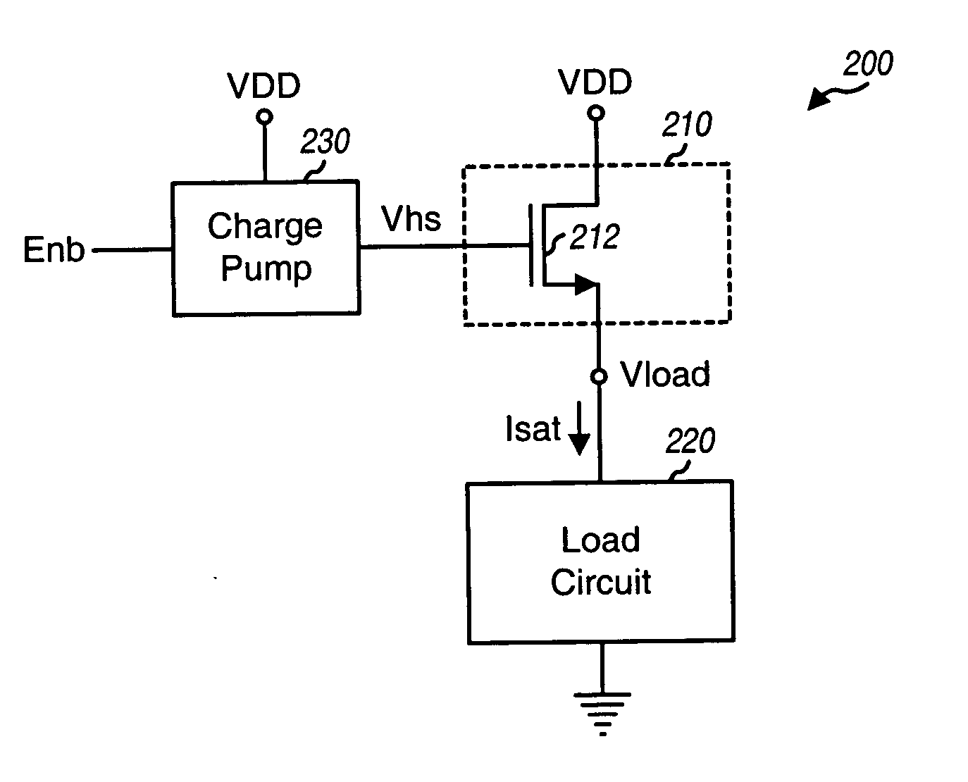
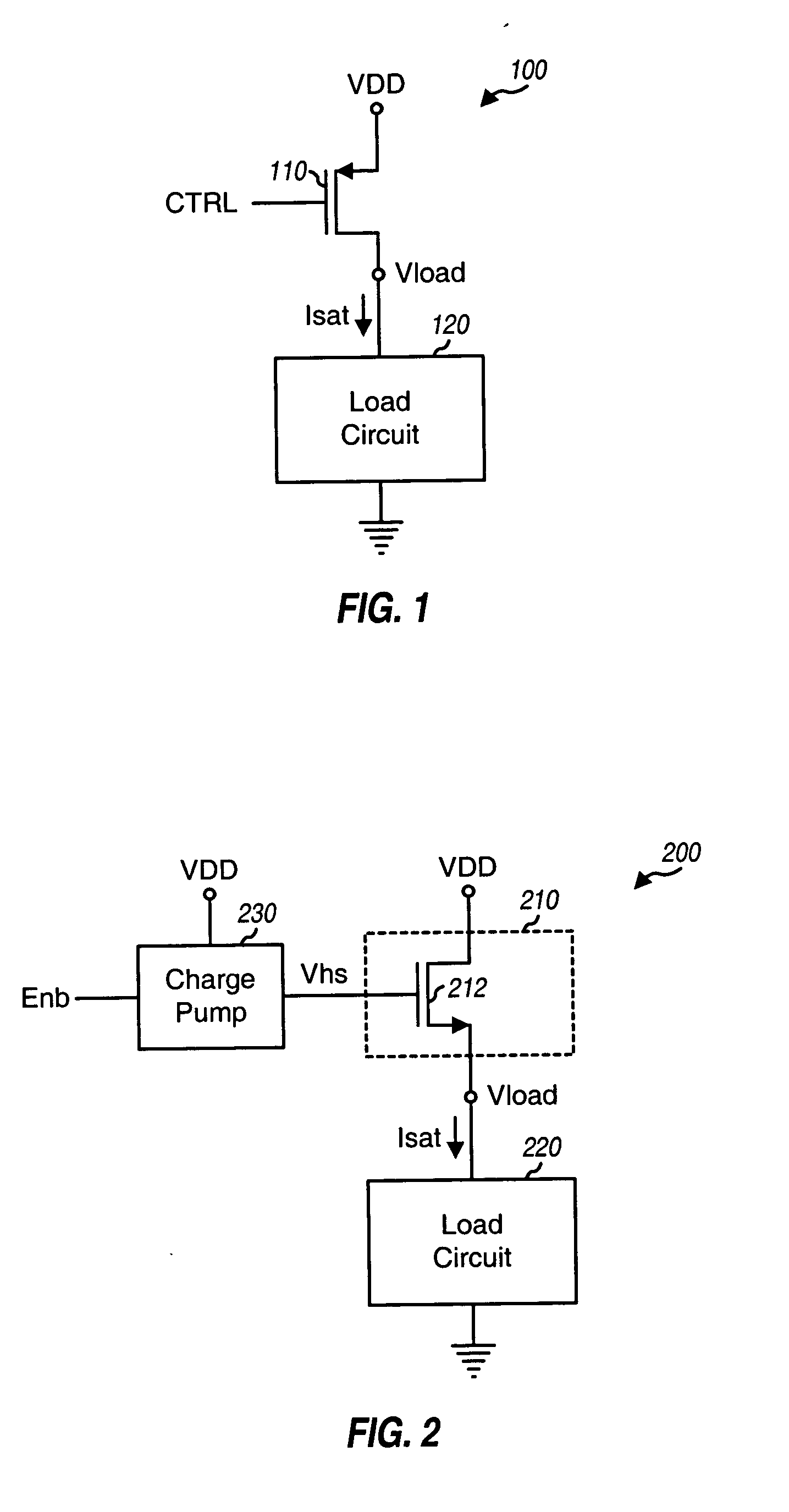
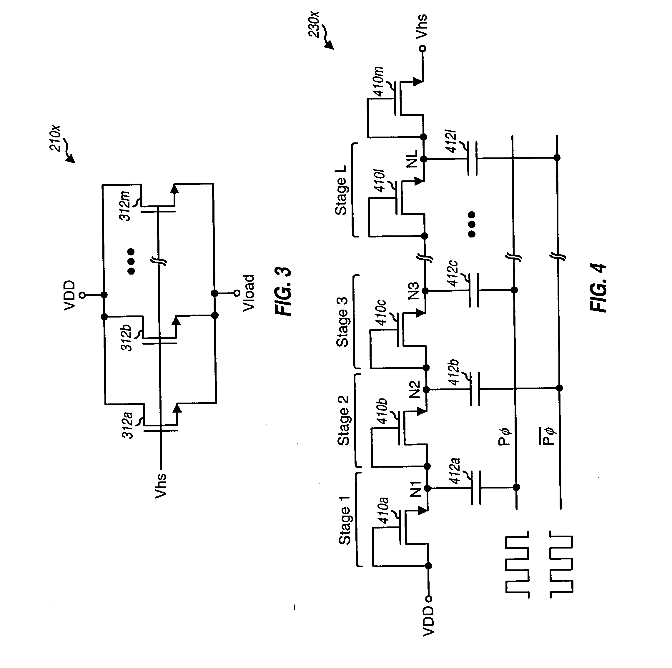
FIG. 1 shows a schematic diagram of an electronic circuit 100 with a conventional P-FET headswitch. Circuit 100 includes a P-FET device 110 coupled to a load circuit 120. P-FET device 110 implements the P-FET headswitch. P-FET device 110 has a source that couples to a power supply, VDD, a gate that receives a control signal CTRL, and a drain that provides a load supply, Vload. Load circuit 120 couples between the load supply and circuit ground.

As used herein, a “load circuit” is a circuit comprised of at least one FET device (i.e., N-FET and / or P-FET devices) and configured to receive power via a headswitch. The load circuit is powered on when the headswitch is enabled and powered off when the headswitch is disabled. The load circui...


PUM


Abstract

An N-FET headswitch has improved performance (e.g., less leakage current, lower ON resistance, and smaller area) over a conventional P-FET headswitch. The N-FET headswitch includes at least one N-FET device and couples between a power supply and a load circuit, which may be, e.g., a microprocessor, a digital signal processor, or a memory unit. The headswitch couples the power supply to the load circuit when the headswitch is enabled and cuts off the power supply from the load circuit when disabled. A charge pump couples to the headswitch and provides a control signal. This control signal is sufficiently high when the headswitch is enabled to ensure that the N-FET device operates in a linear region and has a small drain to source voltage drop. The headswitch may be operated as a power switch or in a feedback configuration to implement a linear or a digital voltage regulator.

Description

BACKGROUND I. Field The present invention relates generally to circuits, and more specifically to a power headswitch. II. Background Integrated circuit (IC) fabrication technology continually improves and, as a result, the size of transistors continues to shrink. This enables more transistors and more complicated circuits to be fabricated on an IC die or, alternatively, a smaller die to be used for a given circuit. Smaller transistor size also supports faster operating speed and provides other benefits. For complementary metal oxide semiconductor (CMOS) technology, which is widely used for digital circuits and some analog circuits, a major issue with shrinking transistor size is standby power. A smaller transistor geometry results in higher electric field (E-field), which stresses a transistor and causes oxide breakdown. To decrease the E-field, a lower power supply voltage is often used for smaller geometry transistors. Unfortunately, the lower power supply voltage also increa...

Claims


Application Information

Patent Timeline
Patent Type & Authority Applications(United States)
IPC IPC(8): H03K17/06
CPCH03K17/063H03K17/06
Inventor FAHIM, AMR
Owner QUALCOMM INC
Why Eureka
Try Eureka