
Process and manufacturing tool architecture for use in the manufacture of one or more protected metallization structures on a workpiece

Inactive Publication Date: 2005-05-03
SEMITOOL INC
View PDF3 Cites 5 Cited by
  • Summary
  • Abstract
  • Description
  • Claims
  • Application Information

AI Technical Summary

Benefits of technology

[0013]A tool architecture for implementing the foregoing process is also set forth. The disclosed tool architecture may be used to minimize the number of wafer movements between the tool sets required to form a complete metallization layer structure.
[0014]The present invention provides a process and corresponding processing tool architecture that facilitates the implementation of efficient and economically viable large-scale manufacturing processes for use in making workpieces, wherein each workpiece has protected copper conductive elements disposed exterior to a barrier layer of the workpiece. The process and tool architecture, although applicable to a wide range of workpiece applications (semiconductor workpiece applications as well as non-semiconductor workpiece applications), are particularly suitable for use in the manufacture of one or more metallization levels of a semiconductor integrated circuit. In the particular embodiment of the process and tool architecture disclosed herein, the resulting protected metallization structure may be readily manufactured using a minimal number of processing tool sets and a minimal number of workpiece movements between the tool sets.

Problems solved by technology

Delays in propagation of electrical signals between devices on a single dice limit the performance of integrated circuits.
More particularly, these delays limit the speed at which an integrated circuit may process these electrical signals.
Larger propagation delays reduce the speed at which the integrated circuit may process the electrical signals, while smaller propagation delays increase this speed.
Diffusion of copper is one such problem.
Such copper diffusion causes failure of devices formed within the silicon.
Another problem is the propensity of copper to oxidize rapidly when immersed in aqueous solutions or when exposed to an oxygen-containing atmosphere.
Oxidized surfaces of the copper are rendered non-conductive and thereby limit the current carrying capability of a given conductor path when compared to a similarly dimensioned non-oxidized copper path.
Existing processes for manufacturing such metallization layers are inefficient and are not economically viable for use in large-scale manufacturing operations.

Method used


Image

  • Process and manufacturing tool architecture for use in the manufacture of one or more protected metallization structures on a workpiece
  • Process and manufacturing tool architecture for use in the manufacture of one or more protected metallization structures on a workpiece
  • Process and manufacturing tool architecture for use in the manufacture of one or more protected metallization structures on a workpiece

Examples


Embodiment Construction

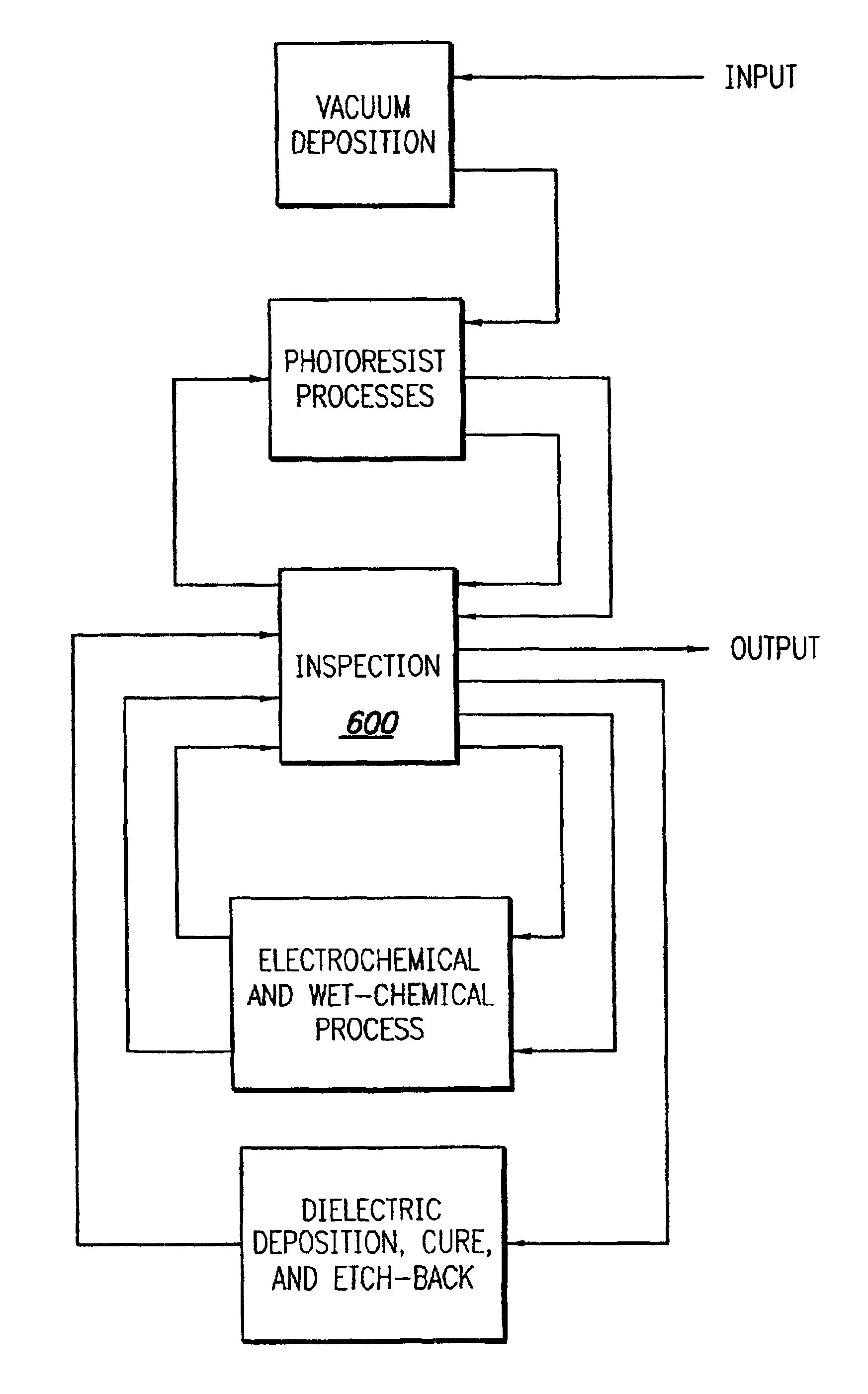
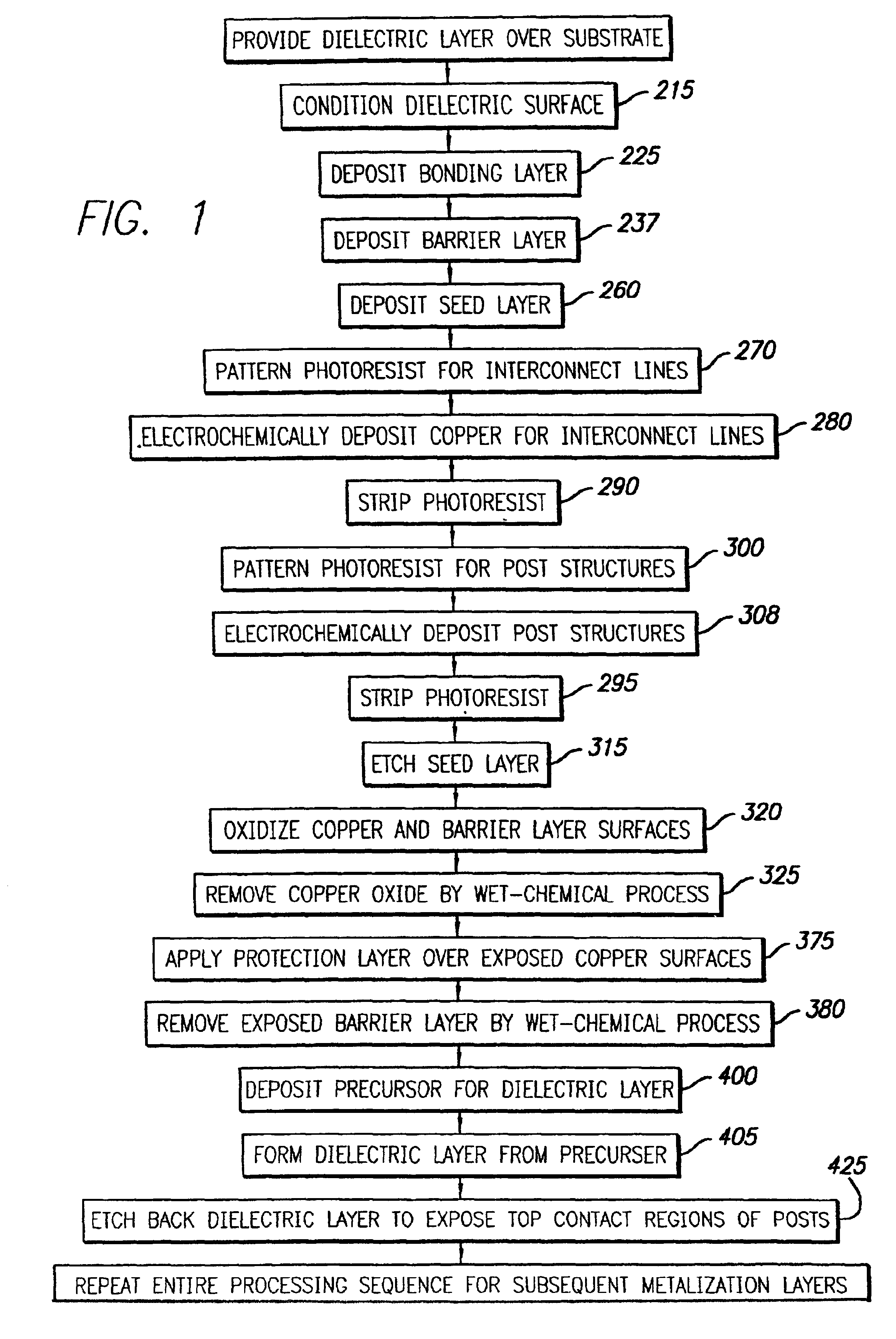
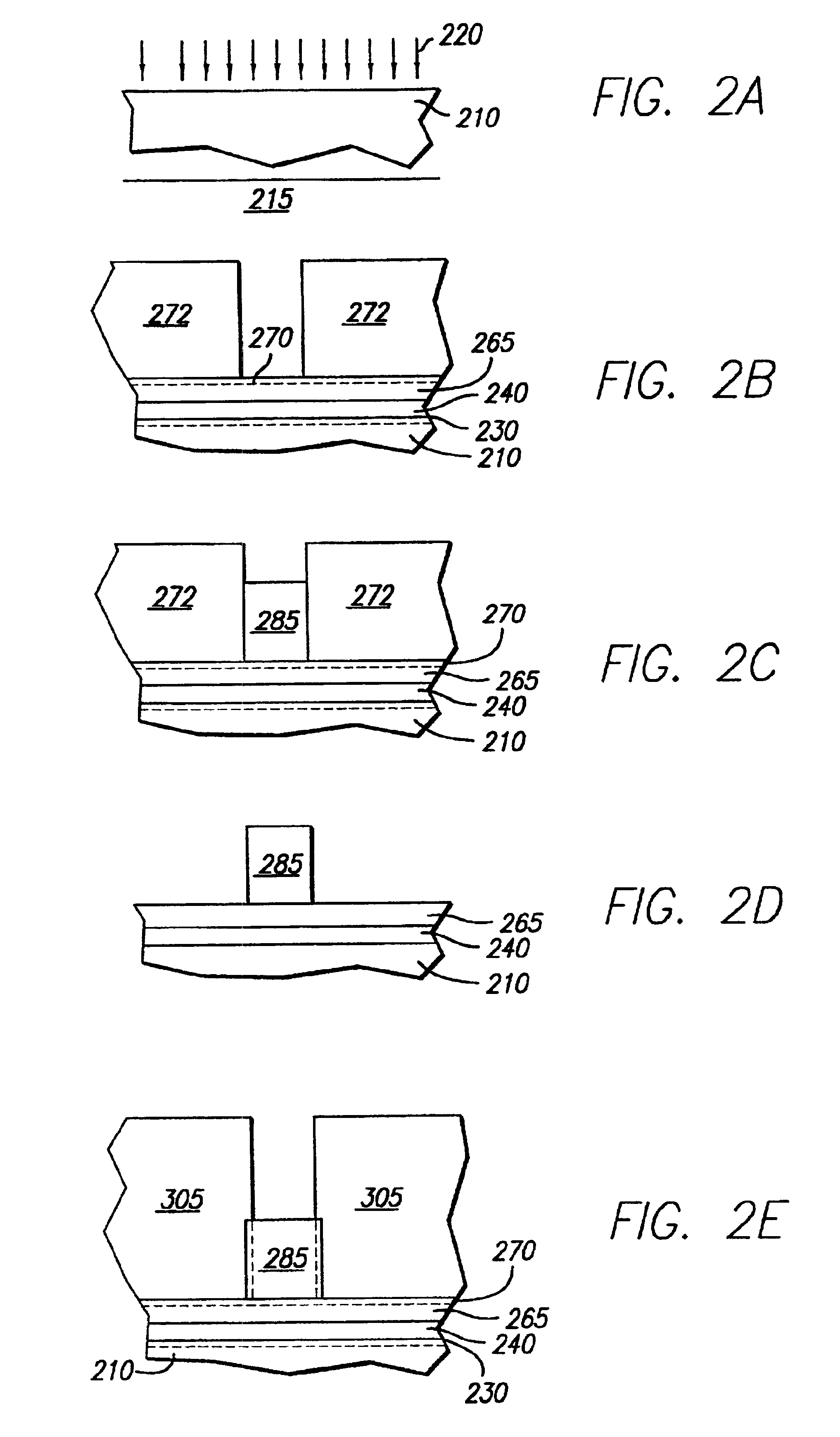
[0020]A basic understanding of certain terms used herein will assist the reader in understanding the disclosed subject matter. To this end, basic definitions of certain terms, as used in the present disclosure, are set forth below.[0021]Single Metallization Level is defined as a composite level of a workpiece that is exterior to the substrate. The composite level comprises one or more interconnect lines and one or more interconnect posts that are substantially covered by a dielectric layer so that the dielectric layer insulates selected interconnect lines and interconnect posts that are not designed to be interconnected from one another.[0022]Substrate is defined as a base layer of material over which one or more metallization levels are disposed. The substrate may be, for example, a semiconductor wafer, a ceramic block, etc.[0023]Workpiece is defined as an object that at least comprises a substrate, and may include further layers of material or manufactured components, such as one ...


PUM

PropertyMeasurementUnit
Electrical conductoraaaaaaaaaa

Abstract

A process for providing one or more protected copper elements on a surface of a workpiece is set forth. In accordance with the process, a barrier layer is applied to the workpiece. If the barrier layer is not suitable as a seed layer for subsequent electroplating processes, a separate seed layer is applied over the surface of the barrier layer. One or more copper elements are then electroplated on selected portions of the seed layer or, if suitable, the barrier layer. If used, the seed layer is then substantially removed. At least a portion of a surface of the barrier layer is rendered unplatable while leaving the copper elements suitable for electroplating. A protective layer is then electroplated onto surfaces of the one or more copper elements.

Description

CROSS-REFERENCES TO RELATED APPLICATIONS[0001]This application is a continuation of U.S. patent application Ser. No. 09 / 076,565, filed on May 12, 1998, and issued as U.S. Pat. No. 6,376,374 B1.STATEMENT REGARDING FEDERALLY SPONSERED "RESEARCH OR DEVELOPMENT"[0002]Not ApplicableBACKGROUND OF THE INVENTION[0003]An integrated circuit is an interconnected ensemble of devices formed within a semiconductor material and within a dielectric material that overlies a surface of the semiconductor material. Devices which may be formed within the semiconductor material include MOS transistors, bipolar transistors, diodes and diffused resistors. Devices which may be formed within the dielectric include thin-film resistors and capacitors. Typically, more than 100 integrated circuit die (IC chips) are constructed on a single 8 inch diameter silicon wafer. The devices utilized in each dice are interconnected by conductor paths formed within the dielectric. Typically, two or more levels of conductor ...

Claims


Application Information

Patent Timeline
IPC IPC(8): H01L21/02H01L21/70H01L21/768H01L21/3213C25D5/02C25D7/12H01L21/288H01L21/3205
CPCC25D5/022C25D7/123H01L21/32051H01L21/32134H01L21/76801H01L21/76825H01L21/76834H01L21/76838H01L21/76852H01L21/76855H01L21/76856H01L21/76873H01L21/76885H01L21/76888H01L21/2885H01L21/76897
Inventor STEVENS, E. HENRY
Owner SEMITOOL INC
Features
  • Generate Ideas
  • Intellectual Property
  • Life Sciences
  • Materials
  • Tech Scout
  • Unparalleled Data Quality
  • Higher Quality Content
  • 60% Fewer Hallucinations
Learn More