Voltage level shifting circuit with improved switching speed

a switching speed and voltage level technology, applied in logic circuits, pulse automatic control, pulse techniques, etc., can solve the problems of less than satisfactory slew rate, affecting transistor switching speed, and the size of sourcing and sinking transistors cannot be simultaneously optimal for both the 1 to 0 and 0 to 1 transitions, so as to achieve the effect of improving the slew ra

Inactive Publication Date: 2005-05-03
MICRON TECH INC
View PDF18 Cites 25 Cited by
  • Summary
  • Abstract
  • Description
  • Claims
  • Application Information

AI Technical Summary

Benefits of technology

[0007]It is an object of this invention to provide a vo

Problems solved by technology

However, because the sizes of sourcing and sinking output drive transistors in known voltage level shifting circuits are often balanced to ensure comparable, if not equal, transition times for both the “0 to 1” and “1 to 0” output transitions, the resulting simultaneous charging and discharging o

Method used


Image

  • Voltage level shifting circuit with improved switching speed
  • Voltage level shifting circuit with improved switching speed
  • Voltage level shifting circuit with improved switching speed

Examples


Embodiment Construction

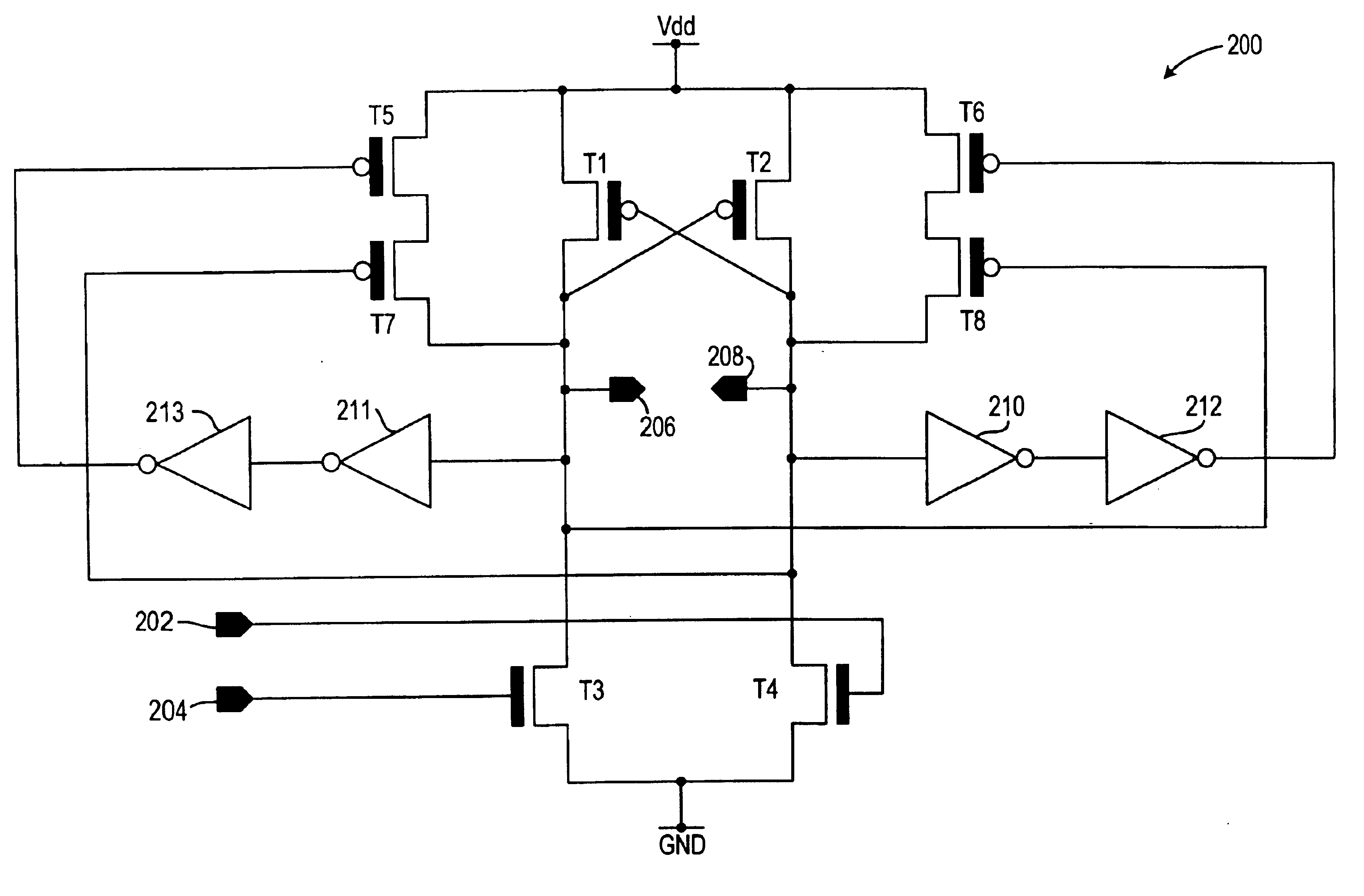
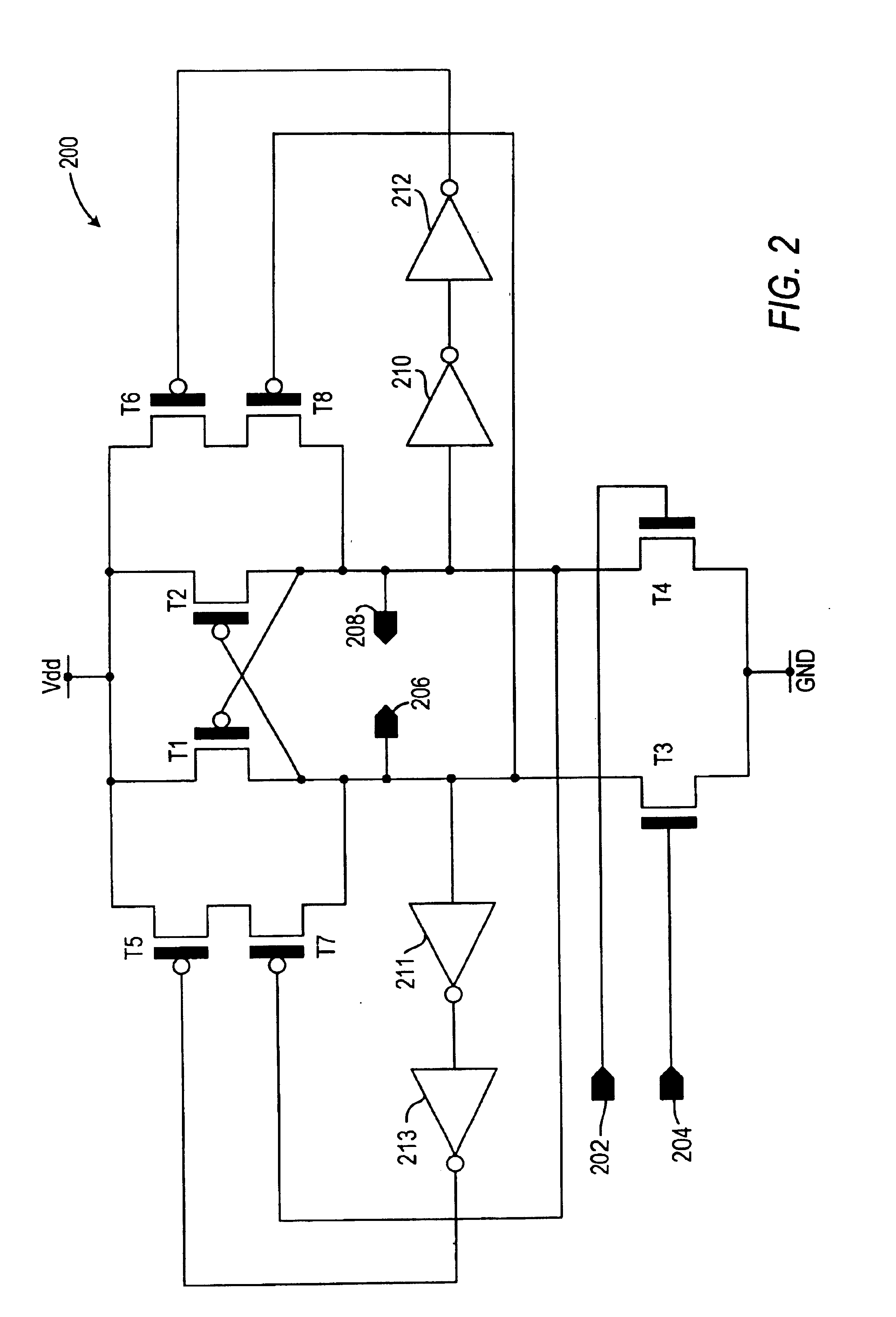
[0015]The invention provides voltage level shifting circuits with improved slew rates. These level shifting circuits include additional circuit devices, such as transistors and inverters, that improve the switching speed of the 0 to 1 output transition, allowing the source and sink output transistors to be sized for improved switching speed of the 1 to 0 output transition.

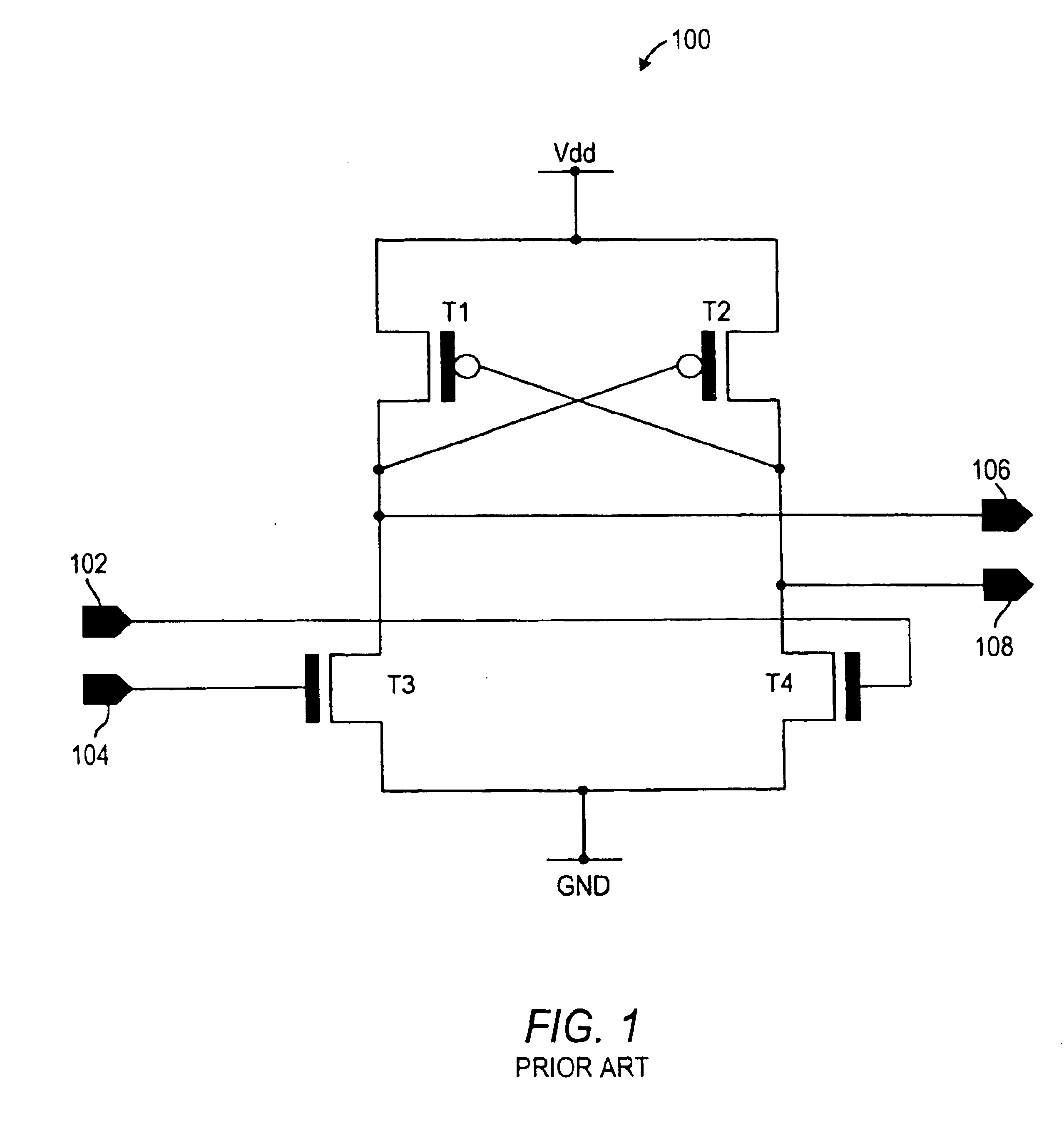
[0016]FIG. 1 shows a known voltage level shifting circuit 100. Circuit 100 includes p-type CMOS devices T1 and T2 and n-type CMOS devices T3 and T4. A p-type CMOS device is “ON” (i.e., it conducts current) when voltage applied to its gate is low (e.g., ground or another logical 0 value) and is “OFF” (i.e., it does not conduct current) when voltage applied to its gate is high (e.g., supply voltage (Vdd) or another logical 1 value). An n-type CMOS device is ON when voltage applied to its gate is high and is OFF when voltage applied to its gate is low. Circuit 100 also includes differential signal input nodes 102 and ...


PUM


Abstract

Voltage level shifting circuits are provided in which circuit devices are placed across sourcing output transistors to improve the switching speed of the low voltage to high voltage output transition. These circuit devices permit sourcing and sinking output transistors to be sized for optimal switching speed of the high voltage to low voltage output transition.

Description

BACKGROUND OF THE INVENTION[0001]This invention relates to voltage level shifting circuits. More particularly, this invention relates to voltage level shifting circuits with improved switching speed.[0002]Voltage level shifting circuits “shift” signaling voltages from one voltage domain to another. For example, core logic in an integrated circuit may operate at 1.6 volts while signaling between integrated circuit chips may require 3.3 volts. In order to maintain proper circuit communication, voltage level shifting circuits provide an interface between these two voltage domains, shifting 1.6 volt signals to 3.3 volt signals and vice versa.[0003]Voltage level shifting circuits typically receive differential input signals and generate differential output signals (that is, they receive two input signals representing opposite logic states and generate two output signals representing opposite logic states). Each output switches from one logic state (or voltage level) to another logic stat...

Claims


Application Information

Patent Timeline
IPC IPC(8): H03K3/356H03K3/00
CPCH03K3/356165H03K3/356113H03K19/01721H03K19/018521
Inventor CLEARY, MARTIN L.HUNT, KENNETH S.
Owner MICRON TECH INC
Why Eureka
Try Eureka