Optical scanning system for surface inspection

Inactive Publication Date: 2005-05-03
KLA TENCOR TECH CORP
View PDF93 Cites 39 Cited by
  • Summary
  • Abstract
  • Description
  • Claims
  • Application Information

AI Technical Summary

Problems solved by technology

A pattern defect may be in or below the plane of the surface and is usually induced by contam

Method used


Image

  • Optical scanning system for surface inspection
  • Optical scanning system for surface inspection
  • Optical scanning system for surface inspection

Examples


Embodiment Construction

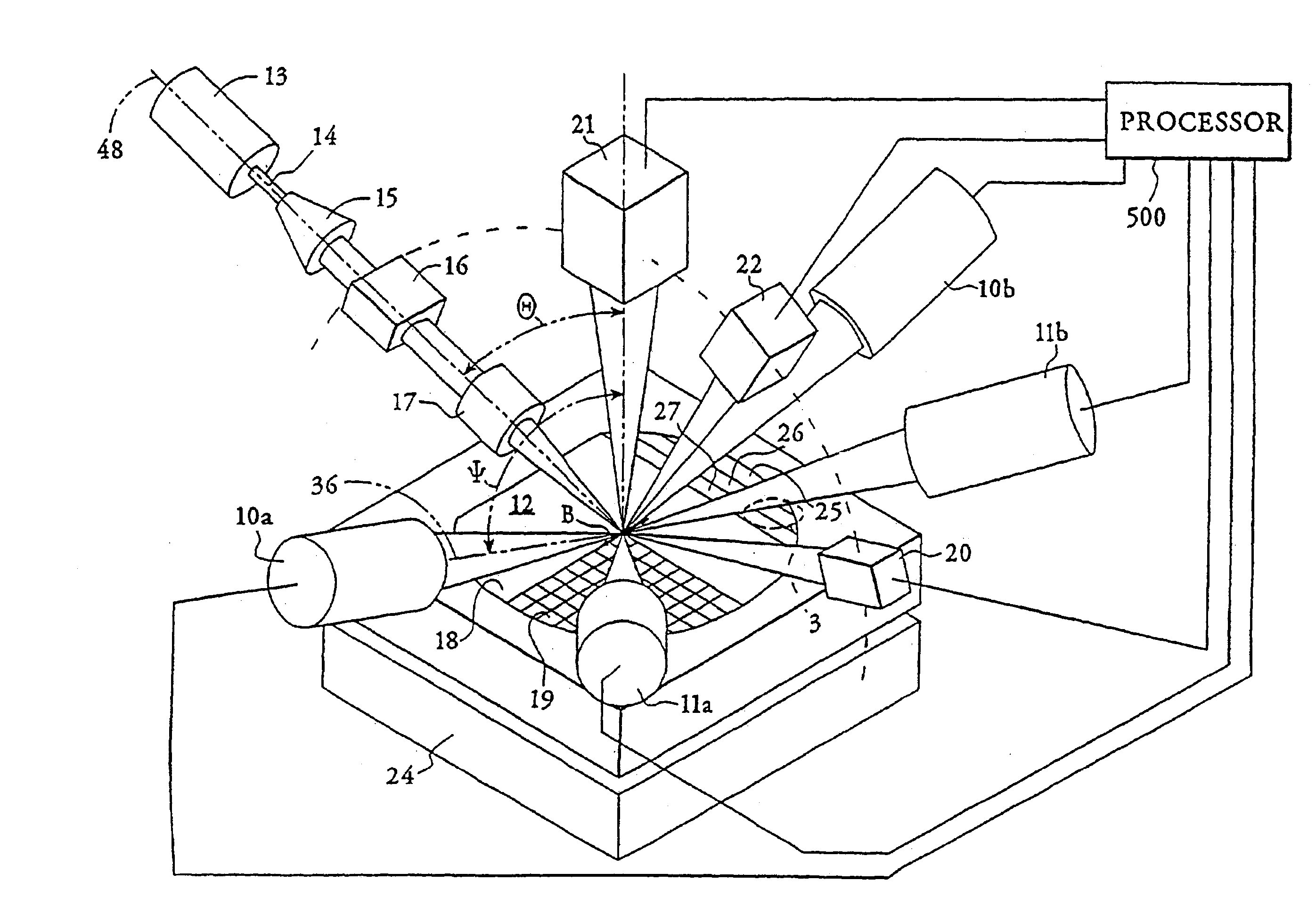
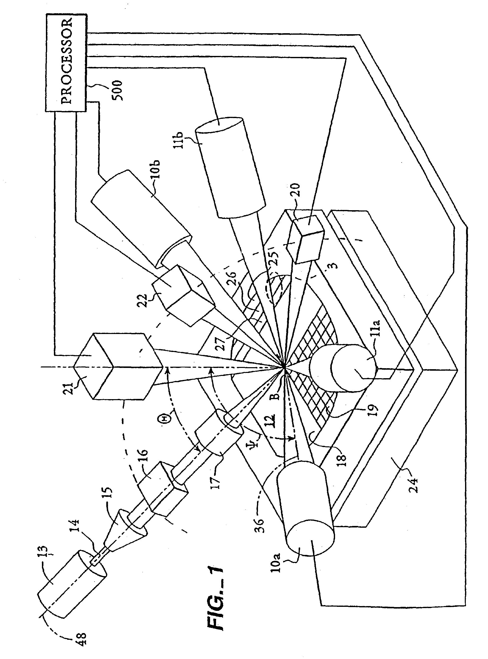
[0034]The present invention, as shown in FIG. 1 is based on the discovery that the scattering cross section of an anomaly on a patterned surface is asymmetrical. This in part is due to the asymmetry of the anomaly itself, or, in the case of particulate contaminants, the pattern on which a particulate rests changing the effective scattering cross section of the particle. Taking advantage of this discovery, a plurality of detectors are provided that includes groups of collector channels symmetrically disposed about the circumference of the surface. Although a greater number of collector channels may be employed in each group, the preferred embodiment uses two groups of two collector channels, 10a-b and 11a-b, disposed symmetrically about the wafer surface 12 so that each collector channel within a pair is located at the same azimuthal angle on opposite sides of the scan line, indicated by the line B. With collector channels positioned symmetrically in the azimuth, a substantial reduct...


PUM


Abstract

In an optical scanning system for detecting particles and pattern defects on a sample surface, a light beam is focused to an illuminated spot on the surface and the spot is scanned across the surface along a scan line. A detector is positioned adjacent to the surface to collect scattered light from the spot where the detector includes a one- or two-dimensional array of sensors. Light scattered from the illuminated spot at each of a plurality of positions along the scan line is focused onto a corresponding sensor in the array. A plurality of detectors symmetrically placed with respect to the illuminating beam detect laterally and forward scattered light from the spot. The spot is scanned over arrays of scan line segments shorter than the dimensions of the surface. A bright field channel enables the adjustment of the height of the sample surface to correct for errors caused by height variations of the surface. Different defect maps provided by the output of the detectors can be compared to identify and classify the defects. The imaging function of the array of sensors combines the advantages of a scanning system and an imaging system while improving signal/background ratio of the system.

Description

[0001]This application is a continuation of U.S. patent application Ser. No. 09 / 571,303, filed May 8, 2000, now abandoned, which is a continuation of U.S. patent application Ser. No. 08 / 868,292, filed Jun. 3, 1997, now U.S. Pat. No. 6,081,325, which claims benefit of Ser. No. 60 / 018,973, filed Jun. 4, 1996.BACKGROUND OF THE INVENTION[0002]The present invention pertains to the field of optical surface inspection. Specifically, the present invention pertains to illumination and light collection optics for inspecting semiconductor wafers and the like.[0003]Monitoring anomalies, such as pattern defects and particulate contamination, during the manufacture of semiconductor wafers is an important factor in increasing production yields. Numerous types of defects and contamination, especially particles, can occur on a wafer's surface. Determining the presence, location and type of an anomaly on the wafer surface can aid in both locating process steps at which the anomaly occurred and determ...

Claims


Application Information

Patent Timeline
IPC IPC(8): G01N21/88G01N21/94G01N21/956
CPCG01N21/94G01N21/95607G01N21/9501
Inventor LESLIE, BRIAN C.NIKOONAHAD, MEHRDADWELLS, KEITH B.
Owner KLA TENCOR TECH CORP
Why Eureka
Try Eureka