Multilayer circuit board and semiconductor device using the same

a multi-layer circuit board and semiconductor technology, applied in the direction of printed circuit aspects, printed circuit non-printed electric components association, electrical apparatus construction details, etc., can solve the problems of insufficient heat dissipation and heat dissipation properties, and achieve the effect of generating a large amount of heat and improving heat dissipation properties

Inactive Publication Date: 2005-05-10
SHINKO ELECTRIC IND CO LTD
View PDF5 Cites 27 Cited by
  • Summary
  • Abstract
  • Description
  • Claims
  • Application Information

AI Technical Summary

Benefits of technology

[0008]It is an object of the invention to solve these problems, and to provide a multilayer circuit board, or a multilayer wiring board, which can have further improved heat-dissipating properties and makes it possible to mount thereon a semiconductor element potentially generating a large amount of heat.

Problems solved by technology

However, even with a multilayer circuit board using a metal sheet for a core substrate, the heat-dissipating properties are not always enough considering the increasing amount of heat generated from a semiconductor element, and a multilayer circuit board having better heat-dissipating properties is required to remove the heat generated from a semiconductor element.
Again, with a multilayer circuit board using such a cover member, heat-dissipating properties are not always enough to increase amount of heat removed from a semiconductor element, and a multilayer circuit board having improved heat-dissipating properties is again required.

Method used


Image

  • Multilayer circuit board and semiconductor device using the same
  • Multilayer circuit board and semiconductor device using the same
  • Multilayer circuit board and semiconductor device using the same

Examples


Embodiment Construction

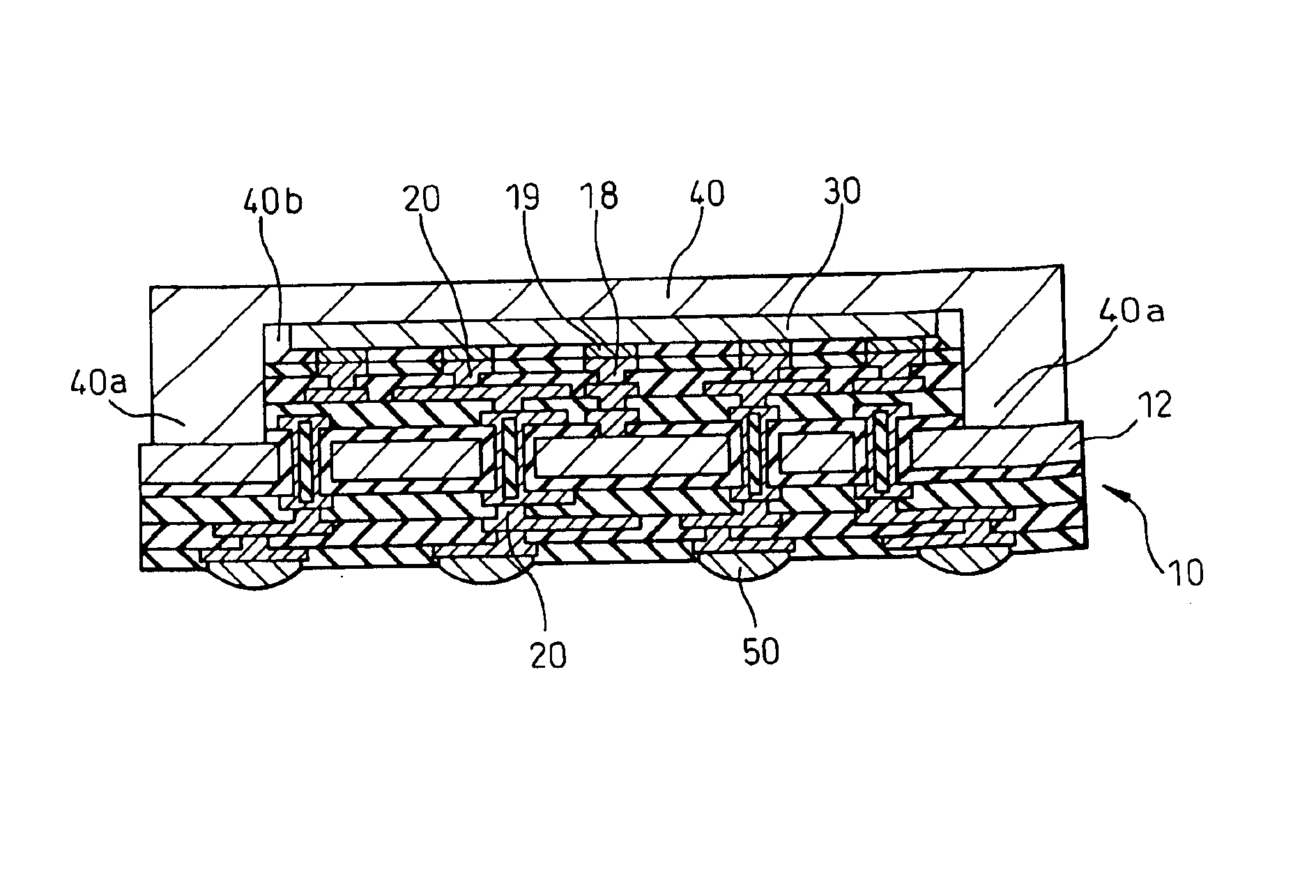
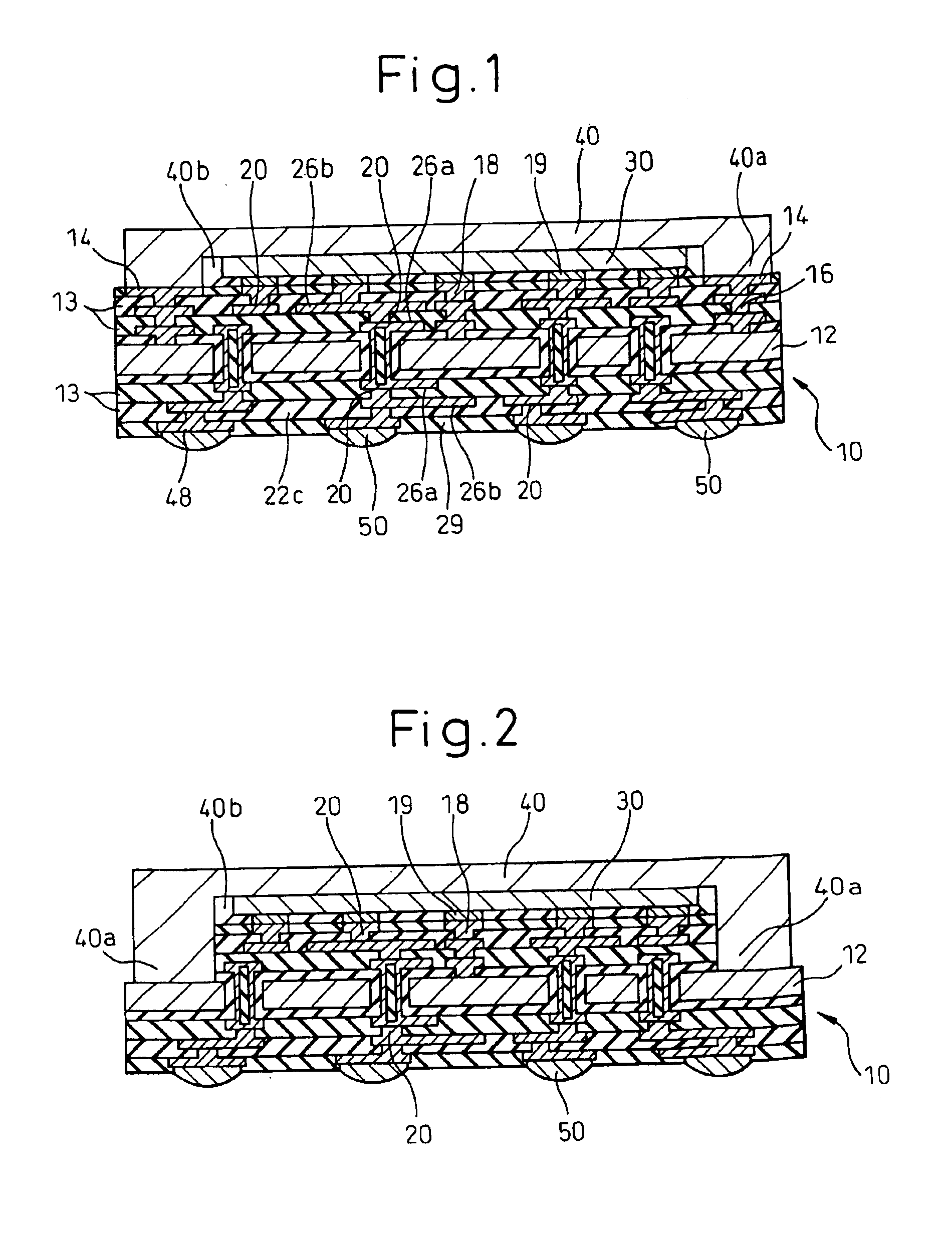
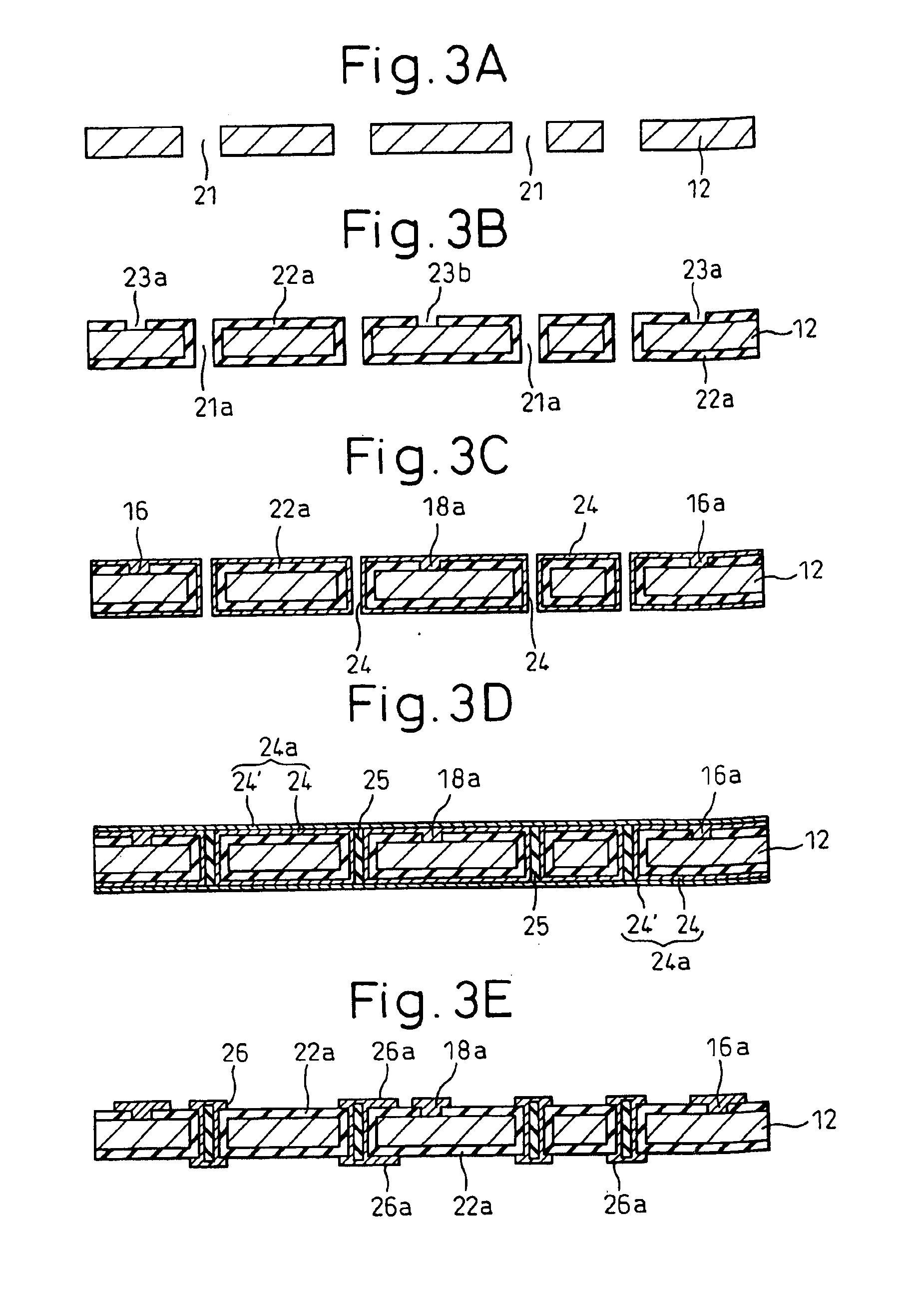
[0024]FIG. 1 shows a sectional view illustrating the structure of a first embodiment of the semiconductor device according to the invention, fabricated by mounting a semiconductor element 30 on the multilayer circuit board 10 of the invention. The multilayer circuit board 10 used in this semiconductor device is formed by stacking a plurality of wiring layers 26a, 26b on either side of a core substrate 12 made of a metal, such as copper or aluminum, each of the stacked wiring layers 26a, 26b being isolated from an adjacent wiring layer by an insulating layer 13 interposed therebetween. The semiconductor element 30 is mounted on one side (the upper side in the drawing) of the multilayer circuit board 10 by flip chip bonding, and has a heat spreader 40 attached so as to cover the semiconductor element 30. The heat spreader is preferably made of a metal, such as copper or aluminum. Wiring patterns 26a, 26b of adjacent wiring layers are connected to each other by a via 20. The multilayer...


PUM


Abstract

A multilayer circuit board for mounting a semiconductor element thereon, comprising a core substrate of a metal material and a plurality of wiring layers stacked on either side of the core substrate, each of the stacked wiring layers being isolated from an adjacent wiring layer by an insulating layer interposed therebetween, the multilayer circuit board having an area at which a heat spreader for dissipating heat generated from the semiconductor element mounted on the circuit board is to be joined to the multilayer circuit board, wherein the multilayer circuit board allows the heat spreader to be joined to the core substrate without the insulating layers being interposed therebetween. A semiconductor device using the multilayer circuit board is also disclosed.

Description

BACKGROUND OF THE INVENTION[0001]1. Field of the Invention[0002]The invention relates to a multilayer circuit board or a multilayer wiring board and a semiconductor device and, more particularly, to a multilayer circuit board having improved heat-dissipating properties and a semiconductor device using it.[0003]2. Description of the Related Art[0004]Among multilayer circuit boards used for semiconductor devices, there are products in which a metal substrate is used as a core substrate, and wiring layers are stacked on either side of the core substrate, each of the stacked wiring layers being isolated from an adjacent wiring layer by an insulating layer interposed therebetween. The stacked wiring layers can be formed on either side of the core substrate by a build-up process. According to a build-up process, a multilayer circuit board, in which one wiring layer is electrically connected to another wiring layer by vias through the insulating layer, can be obtained by forming an insulat...

Claims


Application Information

Patent Timeline
Patent Type & Authority Patents(United States)
IPC IPC(8): H01L23/02H01L23/10H01L23/36H01L23/34H05K1/02H05K3/46H05K3/44H01L23/12H05K1/05H05K1/18
CPCH01L23/10H01L23/36H05K1/0206H01L2224/16H01L2924/01078H05K2201/096H05K3/44H05K3/4608H05K2201/09554H01L2924/15311
Inventor TAKANO, AKIHITOIIJIMA, TAKAHIRO
Owner SHINKO ELECTRIC IND CO LTD
Why Eureka
Try Eureka