ESD protection circuit with plural thyristors

a protection circuit and thyristor technology, applied in semiconductor devices, semiconductor/solid-state device details, transistors, etc., can solve the problems of high parasitic capacitance and more likely transfer of high-frequency noise therebetween, and achieve the effect of suppressing high-frequency nois

Inactive Publication Date: 2005-05-17
RENESAS ELECTRONICS CORP
View PDF3 Cites 7 Cited by
  • Summary
  • Abstract
  • Description
  • Claims
  • Application Information

AI Technical Summary

Benefits of technology

[0017]In accordance with the ESD protection device of the present invention, an ESD stress can be effectively discharged between separate power source lines (such as ground lines) having an equal voltage during the normal operation of the LSI, while suppressing high-frequency noise from transferring between the separate power source lines.

Problems solved by technology

However, the larger dimensions of the diodes constituting the protection devices cause a higher parasitic capacitance between ground line GND1 and ground line GND2, which involves the problem that a high-frequency noise is more likely to transfer therebetween during a normal operation of the LSI.

Method used


Image

  • ESD protection circuit with plural thyristors
  • ESD protection circuit with plural thyristors
  • ESD protection circuit with plural thyristors

Examples


Embodiment Construction

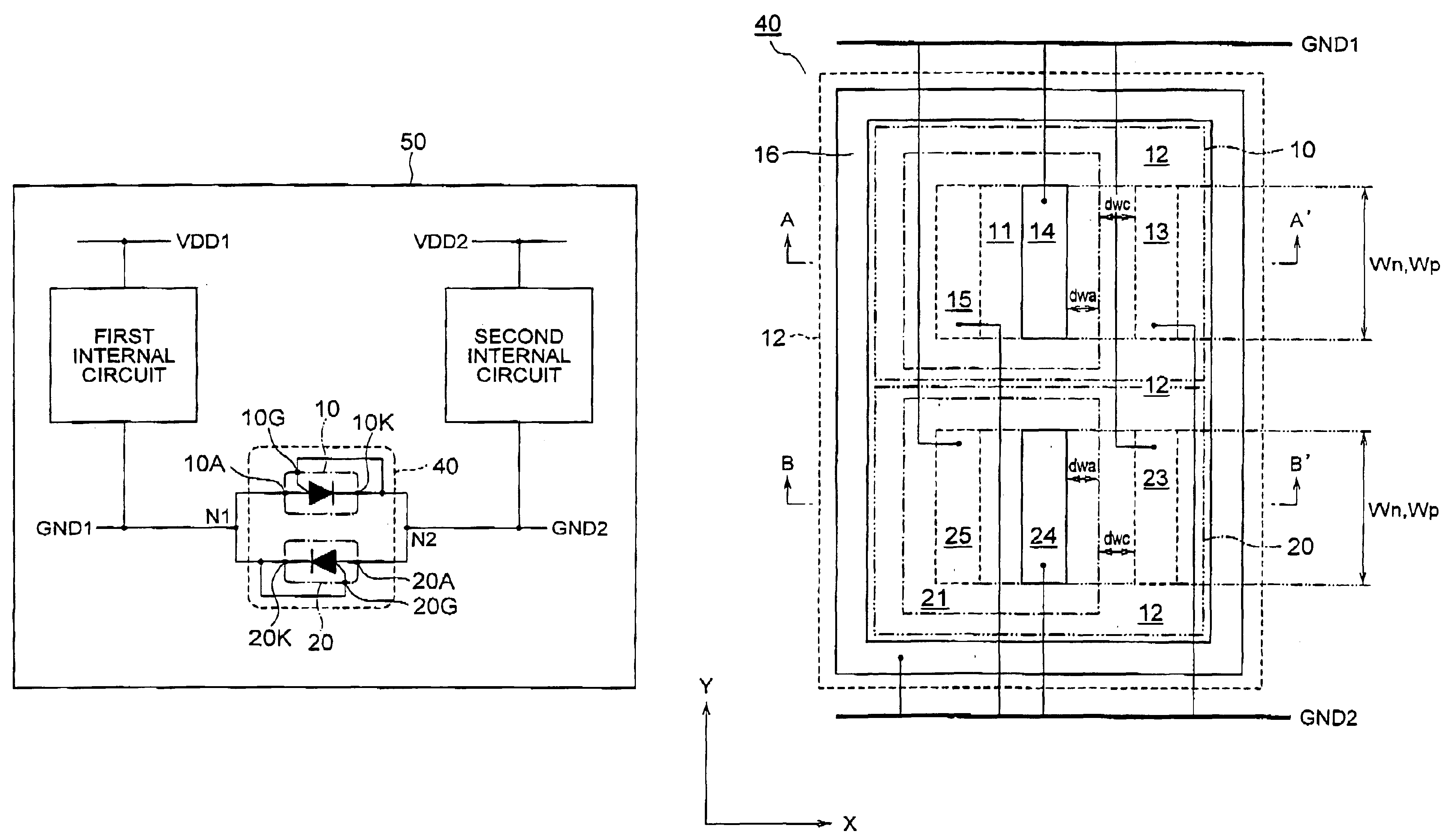
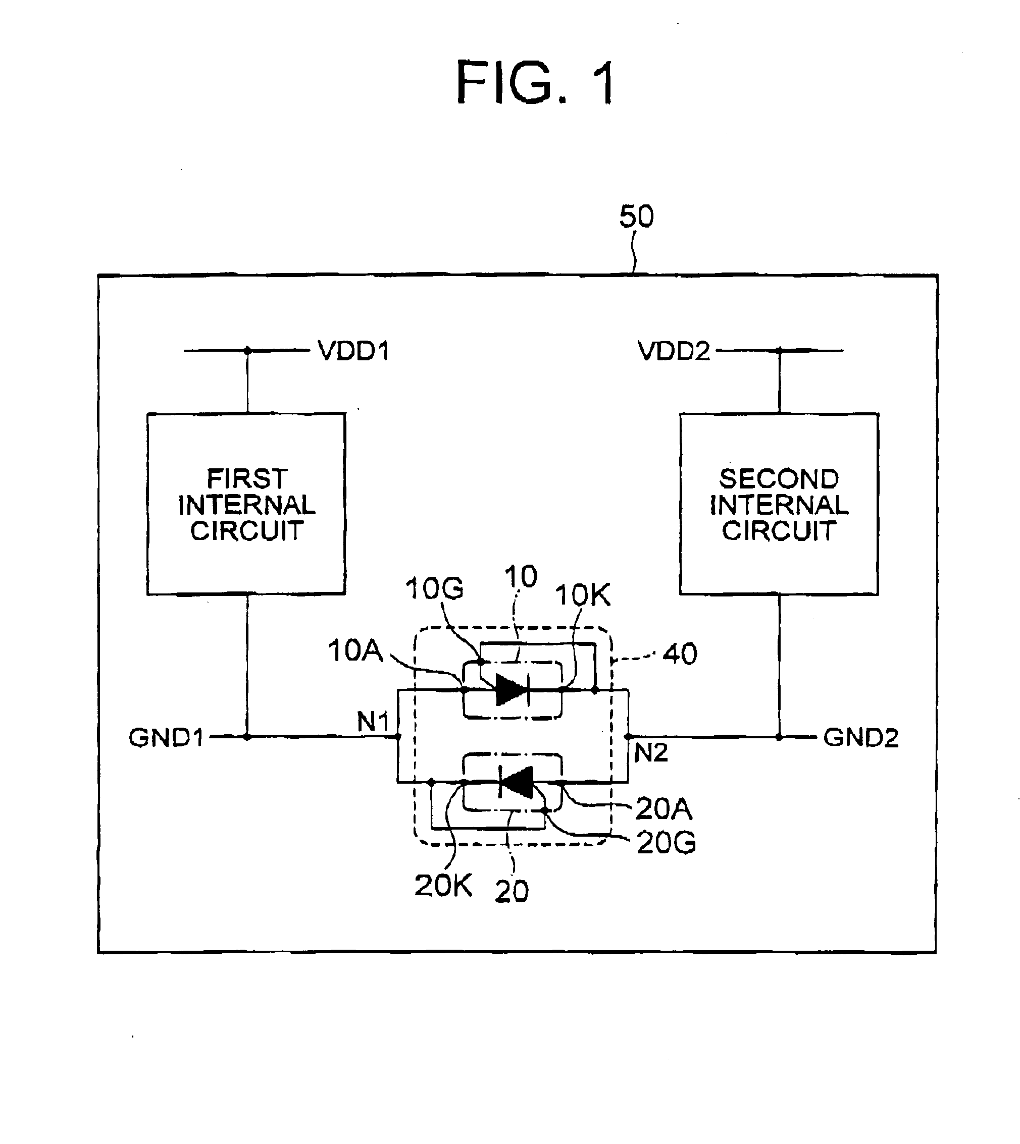
[0032]Referring to FIG. 1, there is shown an equivalent circuit of an LSI including an ESD protection circuit according to a first embodiment of the present invention, which is connected between the ground lines of two different power source systems. The LSI 15 shown in FIG. 1 includes a first internal circuit driven by a first power source system having a high-potential source line VDD1 and a low-potential source line, or ground line GND1, and a second internal circuit driven by a second power source system having a high-potential source line VDD2 and a ground line GND2, wherein ground line GND1 and GND2 are connected to first and second ground terminals, respectively. The ESD protection circuit 40 of the present embodiment is connected between ground line GND1 and ground line GND2. The ESD protection circuit 40 includes a thyristor 10 having an anode 10A connected to a first node N1, and a cathode 10K and a gate 10G connected together to a second node N2, and thyristor 20A having ...


PUM


Abstract

A LSI has a plurality of separate power source systems, and an ESD protection circuit connected between ground lines of two of the power source systems. The protection circuit includes a pair of thyristors connected parallel to one another in opposite directions between the ground lines.

Description

BACKGROUND OF THE INVENTION[0001](a) Field of the Invention[0002]The present invention relates to an electrostatic discharge (ESD) protection circuit and, more particularly, to an ESD protection circuit used in a semiconductor device having a plurality of power source systems isolated from one another.[0003](b) Description of the Related Art[0004]A semiconductor device (hereinafter referred to as LSI) may have a plurality of power source systems therein for use in different internal circuits. For example, in a LSI including an analog circuit and a digital circuit in a single LSI chip, separate power source lines and separate ground lines are used for the analog circuit and the digital circuit to prevent the power source voltage for the analog circuit from fluctuating due to the operations in the digital circuit, in consideration that the analog circuit is more susceptible to the voltage fluctuation.[0005]On the other hand, in a LSI having therein a memory circuit and a CMOS buffer c...

Claims


Application Information

Patent Timeline
Patent Type & Authority Patents(United States)
IPC IPC(8): H01L27/02H01L29/74H01L21/822H01L27/04H01L27/06
CPCH01L27/0262H01L27/04
Inventor MORISHITA, YASUYUKI
Owner RENESAS ELECTRONICS CORP
Why Eureka
Try Eureka