High-speed fully-differential noise reduction device for CMOS optical receivers

A noise reduction, optical receiver technology, applied in electromagnetic receivers, electromagnetic wave transmission systems, electrical components, etc., can solve problems such as the inability to meet the requirements of sensitivity, reduce the equivalent input noise current, maintain bandwidth, reduce The effect of chip area

Inactive Publication Date: 2016-04-06
TIANJIN UNIV
View PDF3 Cites 6 Cited by
  • Summary
  • Abstract
  • Description
  • Claims
  • Application Information

AI Technical Summary

Problems solved by technology

[0005] As one of the key parameters of the optical receiver, the sensitivity is closely related to the noise of the analog front-end circuit, so it is equally important to study the noise reduction technology of the high-speed optical receiver, but there is no good application in the CMOS optical receiver in the prior art The noise reduction device cannot meet the sensitivity requirements in practical applications

Method used


Image

  • High-speed fully-differential noise reduction device for CMOS optical receivers
  • High-speed fully-differential noise reduction device for CMOS optical receivers
  • High-speed fully-differential noise reduction device for CMOS optical receivers

Examples


Embodiment 1

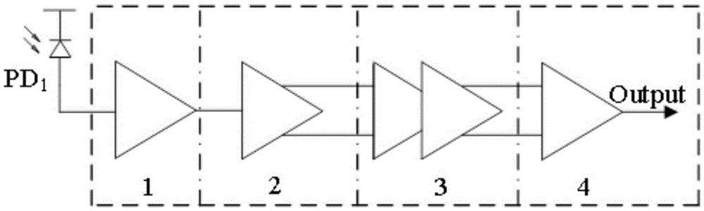
[0037] High-speed fully differential noise reduction device for CMOS optical receivers, see figure 1 , the noise reduction device includes:

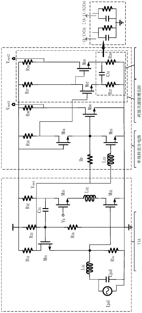
[0038] A low-noise transimpedance amplifier 1 (TIA), which is used to convert the current signal output by the photodetector into a voltage signal, and perform preliminary amplification, and the transimpedance amplifier has a lower equivalent input noise current;

[0039] A single-ended to differential circuit 2 is used to realize single-ended to differential output conversion. While improving the circuit bandwidth and amplifying the voltage signal, this structure can effectively reduce the equivalent input noise current introduced by the back-end circuit;

[0040] A two-stage third-order differential limiting amplifier 3, which uses an interleaved active feedback and capacitive degeneracy circuit, for amplifying the voltage signal to the voltage level required by the digital processing unit;

[0041] An output buffer stage 4 is used to...

Embodiment 2

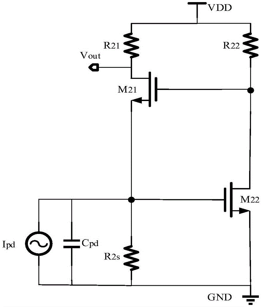
[0049] The following is a simple analysis of the noise of the traditional RGC transimpedance amplifier, and then a detailed description of the working principle of the new RGC transimpedance amplifier from the aspects of expanding bandwidth and reducing noise. As mentioned above, the main purpose of the embodiments of the present invention is to reduce noise. Therefore, the main purpose of expanding bandwidth and single-ended to differential technology is also to reduce noise.

[0050] The embodiment of the present invention comprehensively utilizes the following three technologies to expand the bandwidth, that is, cascode feedback channel reduces input impedance, Miller capacitor "shielding" effect and π-type broadband matching network. And three techniques to reduce noise, that is, a high-pass filter is introduced in the RGC structure, and the inductance L introduced at the input 31 , and introducing an inductance L at the output of the transimpedance amplifier 33 . The p...


PUM


Abstract

The invention discloses a high-speed fully-differential noise reduction device for CMOS optical receivers. The noise reduction device comprises a low-noise trans-impedance amplifier which is used for converting a current signal output by a photoelectric detector into a voltage signal and preliminarily amplifying the voltage signal and has low equivalent input noise current, a single-ended to differential circuit which is used for realizing conversion from single-ended to differential output, increasing the circuit bandwidth, amplifying the voltage signal, effectively reducing equivalent input noise current introduced by a back-end circuit and eliminating common-mode noise introduced by a power supply and the like, a two-stage three-order differential limiting amplifier which adopts a staggered active feedback and capacitance degeneration circuit and is used for amplifying the voltage signal to a voltage level needed for a digital processing unit, and an output buffer stage which is used for converting an output differential voltage signal into a single-ended output voltage signal. On the premise of keeping the overall gain and bandwidth of the circuit, the introduced noise is reduced, and the sensitivity of optical receivers is improved.

Description

technical field [0001] The invention relates to the fields of optical fiber communication systems and optical interconnection, in particular to a high-speed full differential noise reduction device for CMOS optical receivers. Background technique [0002] In today's era of rapid development of network and information technology, the short-distance network communication technology with electrical interconnection as the main connection method gradually shows unavoidable shortcomings, mainly in low speed, large crosstalk, and high power consumption. Optical fiber communication technology can make up for this defect of electrical interconnection with its high speed, no crosstalk and good confidentiality. Therefore, in recent years, the application of optical fiber communication technology in short-distance and very short-distance network communication has attracted extensive attention. For example, between cabinets, between circuit boards and chips, and even between long-distan...

Claims


Application Information

Patent Timeline
Patent Type & Authority Applications(China)
IPC IPC(8): H04B10/69
CPCH04B10/697
Inventor 谢生高谦毛陆虹吴思聪
Owner TIANJIN UNIV
Why Eureka
Try Eureka