Non-volatile semiconductor memory cell utilizing poly-edge discharge
- Summary
- Abstract
- Description
- Claims
- Application Information
AI Technical Summary
Benefits of technology
Problems solved by technology
Method used
Image
Examples
Embodiment Construction
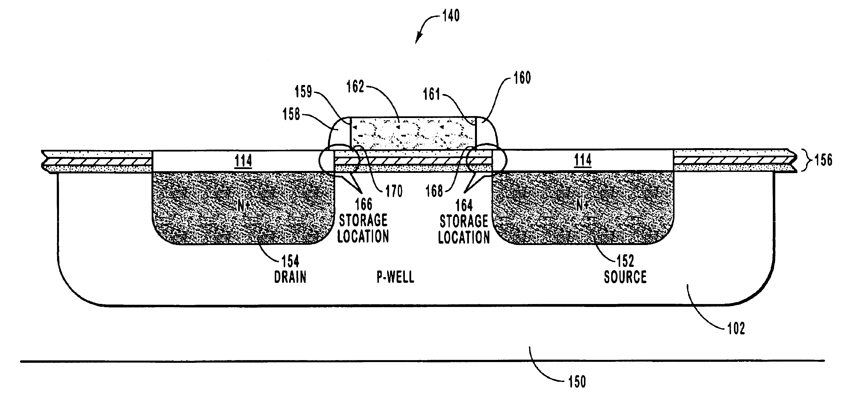
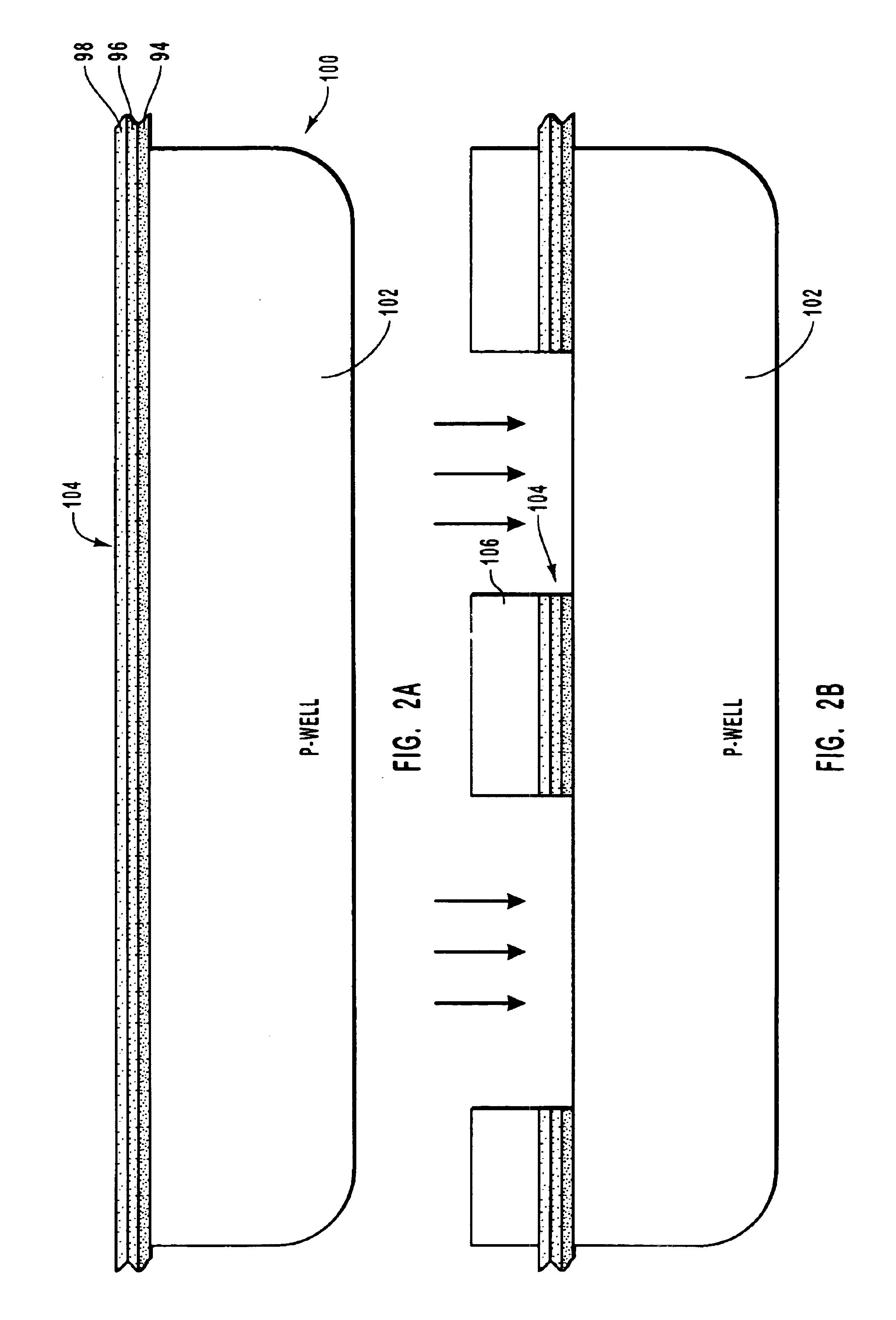
[0021]FIG. 2 depicts the fabrication of a memory cell structure, in accordance with a preferred embodiment of the present invention. In FIG. 2A, a semiconductor substrate 100 is prepared by forming a doped P-well 102 in semiconductor substrate 100. A dielectric composite or trapping region is thereafter developed which consists of a three-layer stack of dielectrics (ONO) 104 consisting of a bottom layer of silicon dioxide 94, a middle layer of silicon nitride (Si3N4) 96, and a top layer of silicon dioxide 98. The outside layers in ONO 104 may either be thermally grown or in the case of the silicon nitride, it may be deposited as a film. While the thicknesses of each component of ONO layer 104 may be varied depending upon the specific process employed, acceptable values for the top layer of oxide 98 may include 90 Å, with the nitride layer 96 assuming a thickness of approximately 20 Å, and the lower level oxide 94 assuming a thickness of approximately 70 Å.
[0022]It should be recalled...
PUM
 Abstract
Description
Claims
Application Information
 - R&D Engineer
- R&D Manager
- IP Professional
- Industry Leading Data Capabilities
- Powerful AI technology
- Patent DNA Extraction
Browse by: Latest US Patents, China's latest patents, Technical Efficacy Thesaurus, Application Domain, Technology Topic, Popular Technical Reports.
© 2024 PatSnap. All rights reserved.Legal|Privacy policy|Modern Slavery Act Transparency Statement|Sitemap|About US| Contact US: help@patsnap.com


