Advances in spike anneal processes for ultra shallow junctions

Inactive Publication Date: 2005-05-24
APPLIED MATERIALS INC
View PDF26 Cites 49 Cited by
  • Summary
  • Abstract
  • Description
  • Claims
  • Application Information

AI Technical Summary

Benefits of technology

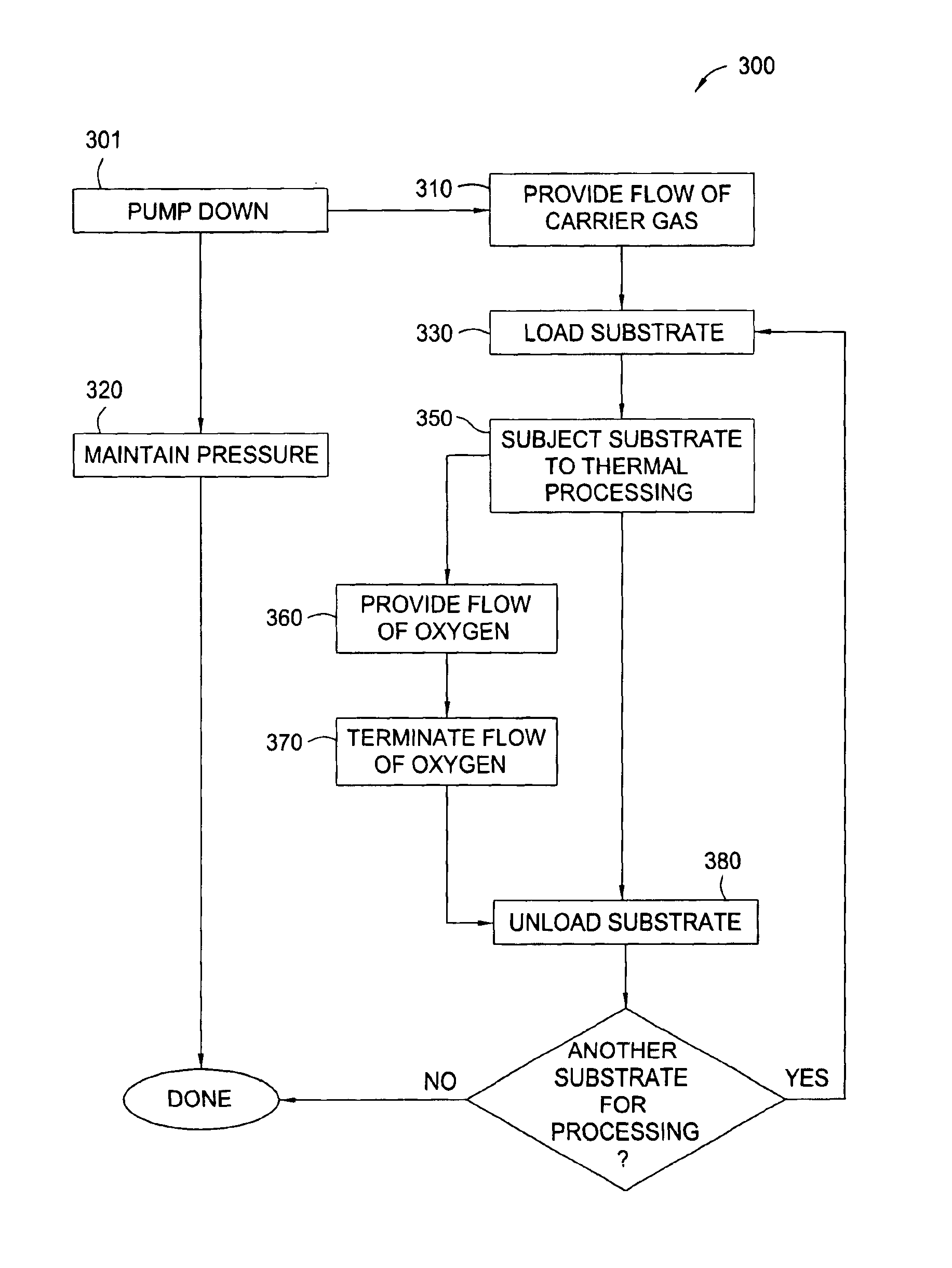
[0011]Significant and surprising improvement in reducing dopant diffusion in ultra shallow junctions was obtained, while maintaining high dopant activation, by providing a flow of a carrier gas into the processing chamber and maintaining gas pressure in the processing chamber below 900 Torr, heating the substrate to a peak temperature above 1000° C., and cooling the substrate at a rate

Problems solved by technology

For example, the presence of oxygen has been found to be necessary in order to decrease the evaporation or out-diffusion of implanted dopants such as boron and arsenic, but too much oxygen in the annealing ambient results in oxygen enhanced diffusion (OED) and limits the creation of shallow junctions, particularly when d

Method used


Image

  • Advances in spike anneal processes for ultra shallow junctions
  • Advances in spike anneal processes for ultra shallow junctions
  • Advances in spike anneal processes for ultra shallow junctions

Examples


examples

[0035]All comparison experiments were performed on B-ion implanted substrates that were pre-amorphised with Ge to reduce deep implants depths and enhance comparison of implant depths.

[0036]B-ion implants were performed using an Applied Materials Quantum™ LEAP implanter. Silicon substrates were pre-amorphised (PAI) with Ge, prior to the B implantation. The Ge pre-amorphisation was optimized for each B implant condition. The B implant energy ranged from 200 to 500 eV, and the implanted dose ranged from 1015 to 2×10¹⁵ atoms / cm2. The initial set of experiments also included 1 keV boron without PAI (dose=1015 atoms / cm2). All boron implants were performed in “decelerated” mode: B ions were extracted at 2 keV and decelerated to the desired final energy level. These substrates were then annealed with varying peak temperatures, using the improved spike profile of FIG. 4. The annealed substrates were measured for sheet resistance and analyzed for junction depth by characterizing boron profile...


PUM


Abstract

Lamp based spike annealing was improved to address the aggressive requirements of <100 nm Ultra Shallow Junction (USJ) technologies. Improvements focused on enhancing cool down rates, and thereby improving spike sharpness. Boron ion implanted substrates with varying ion-implanted energy and dose were then annealed to characterize the improvements in spike annealing. A greater than 10% improvement in sheet resistance and junction depth was realized on substrates that were annealed with the improved spike profile. The improved spike anneal had the same comparable uniformity to the standard spike anneal.

Description

CROSS-REFERENCE TO RELATED APPLICATIONS[0001]This application claims benefit of U.S. provisional patent application Ser. No. 60 / 412,449, filed Sep. 20, 2002, which is herein incorporated by reference. This application is also related to U.S. patent applications Ser. Nos. 10 / 251,440 [6113], filed Sep. 20, 2002, and Ser. No. 10 / 267,053 [6519], filed Oct. 7, 2002 [6519]. Each of the aforementioned related patent applications is incorporated by reference herein.BACKGROUND OF THE INVENTION[0002]1. Field of the Invention[0003]This application relates to semiconductor processing technologies, and particularly to a method of annealing semiconductor substrates with rapid thermal processing.[0004]2. Description of the Related Art[0005]In today's high speed semiconductor devices, ultra-shallow junctions, low sheet resistance and abrupt lateral junctions are vital to reduce short channel effects and to increase transistor saturation current in source drain extensions. Several techniques have be...

Claims


Application Information

Patent Timeline
IPC IPC(8): H01L21/02H01L21/268H01L21/324H01L21/265H01L21/00
CPCH01L21/2686H01L21/324H01L21/26513H01L21/67115H01L21/67109
Inventor RAMACHANDRAN, BALASUBRAMANIANJALLEPALLY, RAVIBOAS, RYAN C.RAMAMURTHY, SUNDARAL-BAYATI, AMIRGRAOUI, HOUDASPEAR, JOSEPH M.
Owner APPLIED MATERIALS INC
Why Eureka
Try Eureka